

Solid State Flash memory is available using NAND and NOR technology. NOR technology allows direct random addressing and data flow in the same way that a normal RAM memory chip does, permitting it to be used for program storage and execution within a processing system. NOR Flash chips are slower, less dense, and have a limited rewrite endurance capability making them inferior to NAND based solutions when used as an alternative to a rotating disk.
NAND Flash technology is a serial memory just like a disk drive. Data is addressed and stored in blocks rather than as individual addressable bits or bytes. NAND Flash based Solid State Drives are designed to mimic a rotating magnetic disk from the system perspective, offering faster access time and comparable data throughput rates. The main disadvantage of a SSD relative to magnetic disk is data density and cost per megabyte.
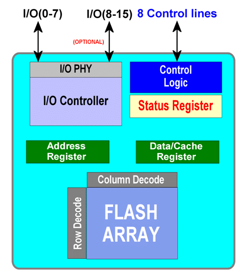
- Data Interface – usually 8 bit, sometimes 16 bit in denser parts
- I/O Controller – Multiplexes data, command, and status word types. Decodes commands
- Control Logic – Manages I/O transaction handshaking with Flash controller
- Address Register – Identifies the block to be accessed for read or write
- Data/Cache register – a single word static register to buffer data between I/O and Array
- Status register – Flags errors in transactions and data flow
- Row/Column Decode – breaks Address value into page values
- Flash Array – the Flash cells arranged in rows and columns
|
Control Line
|
Description
|
Usage
|
|
ALE
|
Input
|
Address latch enable: During the time ALE is HIGH, address information is
transferred from I/O[7:0] into the on-chip address register. Upon a LOW to HIGH
transition on WE#—when address information is not being loaded—the ALE signals
should be driven LOW.
|
|
CE#
|
Input
|
Chip enable: Gates transfers between the host system and the NAND Flash device.
After the device becomes busy or starts a PROGRAM or ERASE operation, CE# can be
de-asserted. See “Bus Operation” on page 16 for additional operational details.
|
|
CLE
|
Input
|
Command latch enable: When CLE is HIGH, information is transferred from
I/O [7:0] to the on-chip command register on the rising edge of WE#. When
command information is not being loaded, the CLE signals should be driven LOW.
|
|
LOCK
|
Input
|
When LOCK is HIGH during power-up, the BLOCK LOCK function is enabled.
To disable BLOCK LOCK, connect LOCK to VSS during power-up, or leave it
unconnected (internal pull-down).
|
|
RE#
|
Input
|
Read enable: Gates transfers from the NAND Flash device to the host system.
|
|
WE#
|
Input
|
Write enable: Gates transfers from the host system to the NAND Flash device.
|
|
WP#
|
Input
|
Write protect: Protects against inadvertent PROGRAM and ERASE operations. All
PROGRAM and ERASE operations are disabled when WP# is LOW.
|
|
I/O[7:0] (x8)
I/O[15:0] (x16)
|
I/O
|
Data inputs/outputs: Bidirectional I/O signals transfer address, data and instruction
information. Data is output only during READ operations; at other times the I/O
signals are inputs.
|
|
R/B#
|
Output
|
Ready/busy: The ready/busy signal is an open-drain, active-LOW output, that uses an
external pull-up resistor. The signal is used to indicate when the chip is processing a
PROGRAM or ERASE operation. The signal is also used during READ operations to
indicate when data is being transferred from the array into the serial data register.
When these operations have completed, the ready/busy signal returns to the high impedance
state.
|
|
VCC
|
Supply
|
VCC: The VCC ball is the power supply.
|
|
VSS
|
Supply
|
VSS: The VSS ball is the ground connection.
|
- Discovery – allows the Flash controller to determine the characteristics of the Flash component
- LUN addressing – allows the controller to activate operations on Flash components independently
- Interleaving – allows the controller to synchronize operations on a set of Flash components
- Caching – allows data to flow to/from controller independent of Flash array operations
- Copyback – allows the Flash component to move data from one block to another without direct controller involvement
- Hynix
- Intel
- Micron
- SanDisk
- Toshiba
- Numonyx (ST Micro)
- Samsung
- Programmatic – cost, schedule, support, warranty, and availability.
- Technical – performance, power, package options, features, scalability, and flexibility.
- Other – commonality, compatibility, documentation, development support, testing, and reputation.


 Amazon