

Today, at the rescheduled GTC (GPU Technology Conference organized by NVIDIA), NVIDIA revealed that they have begun shipping their first 7nm GPU to appliance manufacturers. Much like AMD, who released a 7nm GPU two years ago in 2018, NVIDIA is choosing to focus on the data center use cases for their first 7nm GPU. NVIDIA has been emphasizing developments in artificial intelligence and other high-performance computing. The company even recently bought out Mellanox. Earlier this month, NVIDIA announced they were looking to acquire Cumulus as well.
NVIDIA’s first 7nm GPU is the NVIDIA A100. The A100 is based on NVIDIA’s Ampere architecture and contains 54 billion transistors. Like previous NVIDIA data center GPUs, the A100 includes Tensor Cores. Tensor cores are specialized parts of the GPU designed specifically to quickly perform a type of matrix multiplication and addition calculation commonly used in inferencing.With new beefier GPUs, comes new, beefier Tensor Cores. Previously, NVIDIA’s Tensor Cores could only support up to thirty-two bit floating-point numbers. The A100 supports sixty-four bit floating-point operations, allowing for much greater precision.
Also new in the A100 is a multi-instance GPU capability. Each A100 GPU is capable of splitting into as many as seven independent instances to address a large number of tasks simultaneously.
NVIDIA A100 Specifications
|
Transistor Count |
54 billion |
|
Die Size |
826 mm2 |
|
FP64 CUDA Cores |
3,456 |
|
FP32 CUDA Cores |
6,912 |
|
Tensor Cores |
432 |
|
Streaming Multiprocessors |
108 |
|
FP64 |
9.7 teraFLOPS |
|
FP64 Tensor Core |
19.5 teraFLOPS |
|
FP32 |
19.5 teraFLOPS |
|
TF32 Tensor Core |
156 teraFLOPS | 312 teraFLOPS* |
|
BFLOAT16 Tensor Core |
312 teraFLOPS | 624 teraFLOPS* |
|
FP16 Tensor Core |
312 teraFLOPS | 624 teraFLOPS* |
|
INT8 Tensor Core |
624 TOPS | 1,248 TOPS* |
|
INT4 Tensor Core |
1,248 TOPS | 2,496 TOPS* |
|
GPU Memory |
40 GB |
|
GPU Memory Bandwidth |
1.6 TB/s |
|
Interconnect |
NVLink 600 GB/s PCIe Gen4 64 GB/s |
|
Multi-Instance GPUs |
Various Instance sizes with up to 7MIGs @5GB |
|
Form Factor |
4/8 SXM GPUs in HGX A100 |
|
Max Power |
400W (SXM) |
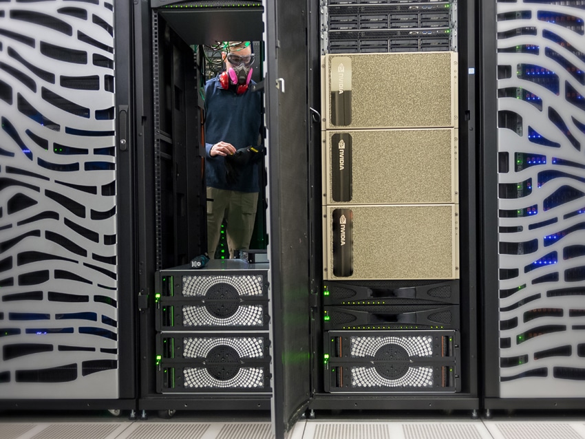
In addition to the single A100 GPU, NVIDIA is simultaneously releasing two clustered GPUs as well. The NVIDIA DGX A100 system features eight NVIDIA A100 GPUs interconnected with NVIDIA NVSwitch. It’s smaller brother, NVIDIA HGX A100 is made up of four A100 GPUs interconnected through NVLink. Both NVLINK and NVSwitch allow the individual GPUs to work together on large tasks. NVLink is a true all-to-all interconnect. In order to handle the larger number of GPUs on the NVSwitch interconnects, NVIDIA settled for cross-connecting the NVLinks between the GPUs together. NVIDIA has beefed up their all-to-all interconnect for the new A100, doubling the connectivity to support the much more powerful cores in the chips. NVIDIA claims that they’ve more than doubled the performance of their previous DGX system. According to them, their new eight GPU DGX A100 can perform an incredible five petaflops. Their previous generation, the DGX-2 sixteen GPUs, but only manages two petaflops. I didn’t expect to be using the word “only” with any system that boasted two petaflops anytime soon, but when the new cluster more than doubles the performance with half the number of GPUs, it seems fitting. The DGX A100 also boasts 320GB of memory and nine NVIDIA Mellanox ConnectX-6 HDR 200Gb per second network interfaces, offering a total of 3.6Tb per second of bi-directional bandwidth.
To put the sheer power of the DGX A100 into perspective, the tenth most powerful supercomputer in the world is benchmarked at 18 petaflops. Shove a couple of NVIDIA’s new bad boys together, and you’ve got your very own world-class supercomputer. Astonishingly, NVIDIA has released a DGX SuperPOD reference architecture which does just that. If the system performs as well as NVIDIA claims, the next few months might be very strange for supercomputing enthusiasts.
Back in the normal world, with more typical use-cases, NVIDIA has also announced plans to release an edge server using their new GPUs by the end of the year. The EGX A100 will be powered by just one of the new A100 GPUs. NVIDIA plans for the EGX A100 edge server to run on Red Hat Enterprise Linux. The appliances will likely use NVIDIA’s recently acquired Mellanox ConnectX-6 Dx network cards to receive up to 200Gbps of data and send it directly to the GPU memory for AI or 5G signal processing. That NVIDIA itself isn’t planning on releasing an appliance with just one of their new GPUs in it until the end of the year really underlines what a wild idea clustering multiple DGX A100s, which themselves are clusters of eight A100s, together, really is.


 Amazon