

Samsung has announced that its 5nm FinFET process technology is now ready for customer samples. Back in October of 2018, they began production of EUV-based 7nm LLP process, its first process node with EUV lithography technology. With the 5nm FinFET process, it provides up to a 25% more in logic area efficiency with 20 percent lower power consumption or 10 percent higher performance. Samsung can reuse the 7nm IP to 5nm as well, which allows its customers transitioning to 5nm to reduce migration costs, have a pre-verified design ecosystem and shorten their 5nm product development. 5nm uses EUV lithography in metal layer patterning and reduces mask layers while providing better fidelity.
The collaboration between Samsung Foundry and its Samsung Advanced Foundry Ecosystem (SAFE) partners enables a “robust design infrastructure” for their 5nm, including the process design kit (PDK), design methodologies (DM), electronic design automation (EDA) tools, and IP. Samsung Foundry has begun offering a 5nm Multi Project Wafer (MPW) service to customers.
Samsung is also working with its customers on 6nm, a customized EUV-based process node, and has received the product tape-out of its first 6nm chip.
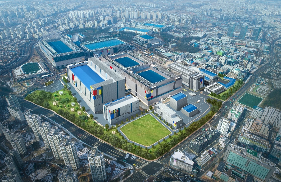
Currently, production of Samsung foundry’s EUV-based process technologies is taking place at the S3-line in Hwaseong, Korea. They are planning an expansion with its EUV capacity to a new EUV line in Hwaseong, which is expected to be completed sometime during the second half of 2019 with a production ramp-up the following year.
Sign up for the StorageReview newsletter


 Amazon