

Samsung announced that is has developed the industry's first high bandwidth memory chip manufactured using 12-layer 3D-TSV (Through Silicon Via) technology. High bandwidth memory (HBM) is used in lots of computer components used in artificial intelligence and machine learning applications like high-end graphics cards, FPGAs, CPUs, and networking devices. Previously, the best anyone could do was 8-layer. Samsung was founded in 1938 and is well known for its electronics products. They've been one of the major drivers in this area for some time. Impressively, this is the second advancement they've made in the HBM area this year; last March, they announced the development of a very high capacity HBM2E chip named Flashbolt with 410GBps data bandwidth and 16GB of memory.
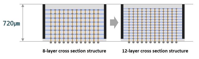
Samsung’s new technology stacks 12 DRAM chips in the same 720㎛thickness as their current 8-layer HBM2 products. Achieving this fifty percent increase in density requires more than sixty thousand TSV holes which presents a significant production challenged and Samsung has been understandably cagey about when exactly these new chips will be available for manufacturers to begin including them in their processing chips. The only thing Samsung has told us so far is that they will be able to mass-produce them soon, suggesting that they have not even finalized the production lines yet. Once manufacturers get their hands on them, it shouldn't take long for them to make their way into consumers' hands since they share the same thickness (and presumably other form factor dimension although Samsung didn't say so), as the current generation of HBM2 memory.
This makes the second advance in HBM2 manufacturing Samsung has made so far in 2019. In March of this year, Samsung announced the development of an HBM2E chip named Flashbolt with twice the memory capacity, 16GB, of the chips currently on market. Combining the advances showcased in Flashbolt with their newest development allowing them to pack half again as many layers into the same space, Samsung is predicting some very impressive numbers for their not yet named next high bandwidth memory chip. Samsung says the new chip will have a 24GB capacity. They have not yet told us what the new bandwidth will be.


 Amazon