

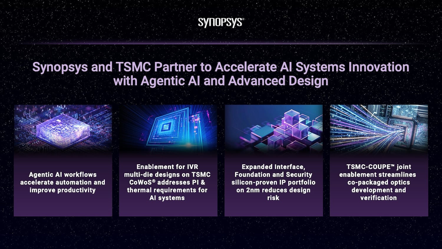
Synopsys har certifierat sina digitala och analoga EDA-flöden på TSMC:s A14-process och slutfört 64G UCIe IP-tape-outs på TSMC:s 2nm- och 3nm-noder, de två hårda milstolparna i en bredare uppsättning gemensamma arbeten som företagen tillkännagav kring TSMC:s Open Innovation Platform-ekosystem. Resten av nyttolasten täcker agentiska AI-designflöden över Synopsys analoga, digitala och multi-die-verktyg, integrerad spänningsregulator-samdesign på CoWoS-kapsling, ett fotoniskt och elektroniskt samdesignflöde för TSMC:s COUPE-sampaketerade optik, och en lista över IP-tape-outs på N2P som inkluderar PCIe 7.0, HBM4, LPDDR6 och 224G Ethernet.
”I takt med att AI-system fortsätter att växa i skala och komplexitet kräver kunderna beprövad IP, intelligenta designlösningar och avancerade paketeringsmetoder som fungerar sömlöst tillsammans”, säger Michael Buehler-Garcia, Senior Vice President på Synopsys. ”Våra gemensamma innovationer med TSMC adresserar det kontinuum av kisel-till-system-samdesignfunktioner som behövs för att påskynda utvecklingen av nästa generations AI och högpresterande datorsystem.”
A14-certifiering och agentdesignflöden
A14-certifieringen sträcker sig från implementering till signering för både digitala och analoga flöden, vilket är vad ett designteam behöver innan de kan genomföra en tape-out till noden. På den analoga sidan arbetar Synopsys och TSMC med enhetsroutingaktivering för A14, vilket Synopsys beskriver som en viktig milstolpe för avancerad analog plats-och-route-automation. Arbetet med agentic AI sker genom tre verktyg: Synopsys Custom Compiler accelererar analog migrering, Fusion Compiler använder LLM-assisterad analys för att öka produktiviteten, och ett nytt agentic chiplet-floorplan-samoptimeringsflöde i Synopsys 3DIC Compiler-plattformen automatiserar floorplanering för heterogena multi-die-designer på TSMC 3DFabric-kapsling.
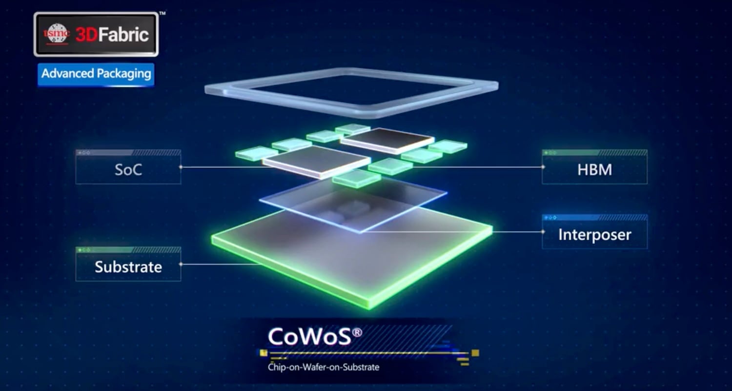
Strömförsörjning och optik får sina egna gemensamma designvägar. 3DIC-kompilatorplattformen låter nu konstruktörer samdesigna och simulera integrerade spänningsregulatorer på TSMC CoWoS i en miljö, vilket Synopsys positionerar som ett sätt att förbättra energieffektivitet och energiintegritet i multi-die-designer i takt med att AI-paket höjer kraven på energiförsörjning. För sampaketerad optik har de två företagen ett integrerat fotoniskt och elektroniskt samdesignflöde för TSMC:s COUPE-teknik som omfattar 3DIC-implementering, multifysikanalys och optimering, så att kunder kan utveckla och verifiera optiska sammankopplingsarkitekturer inuti en multi-die-design.
”Vårt samarbete med ekosystempartners inom Open Innovation Platform (OIP) som Synopsys fortsätter att möta de snabbt växande kraven från AI och högpresterande datoranvändning”, säger Aveek Sarkar, chef för Ecosystem and Alliance Management Division på TSMC. ”Genom att kombinera certifierade EDA-lösningar och en kiselbeprövad IP-portfölj från Synopsys med våra senaste process- och förpackningsinnovationer gör vi det möjligt för kunder att tänja på gränserna för prestanda, integration och energieffektivitet för att forma framtiden för AI.”
UCIe Silicon och N2P IP-listan
På die-to-die-sidan demonstrerade Synopsys UCIe-A 32G/40G-kisel på ett TSMC N3P-testchip integrerat med en CoWoS-S-interposer, och de slutförde nyligen 64G UCIe IP-tapeouts på både 2nm och 3nm, med inbäddad DFT för synlighet i systemet. Det är samma standard som AMD bygger in i Versal RF för chiplet-länkar, och 64 GT/s är den högsta datahastigheten i UCIe 3.0-specifikationen.
Angående TSMC:s N2P-process rapporterar Synopsys milstolpar för IP-aktivering och tape-out för PCIe 7.0, HBM4, LPDDR6/5X/5, 224G Ethernet PHY, UCIe, OTP och Silicon Lifecycle Management-processer, spännings- och temperaturövervaknings-IP. De har också utökat sina kiselbeprövade Foundation-, MIPI- och minnes-IP för N3P och N2P och utvecklar IP för TSMC:s kompakta "C"-processer från 6nm till 3nm. CXL 4.0-IP:n med 128 GT/s som vi behandlade i augusti ligger bredvid denna portfölj.


 Amazon