

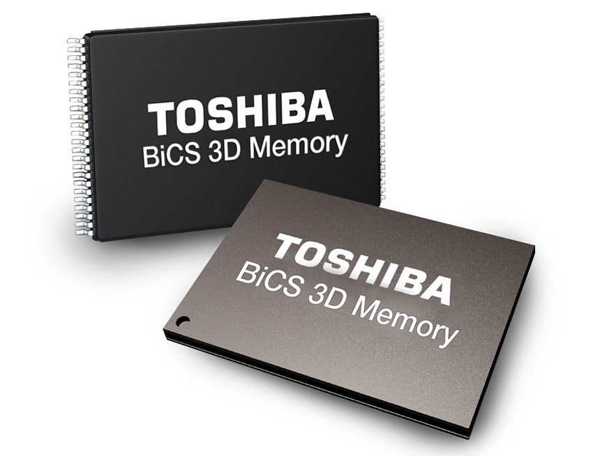
SanDisk has announced the world’s first 256Gb 3-bit-per-cell (TLC) 48-layer 3D NAND chip using BiCS technology as well as the beginning of 3D NAND pilot line operations in Yokkaichi, Japan, in a joint effort with its partner, Toshiba. SanDisk’s 256 Gb X3 BiCS chip is built for wide range of use cases including consumer, client, mobile and enterprise products. Both companies initially announced the development of 48-layer 3D NAND back in late March of this year.
Previously two-bit-per-cell, BiCS is a nonvolatile memory architecture that is designed to provide enhanced levels of density, scalability and performance to flash-based devices. SanDisk also indicates that BiCS NAND memory will noticeably improve write and erase endurance, write speeds, and overall energy efficiency compared to previous, conventional 2D NAND.
Availability
SanDisk’s 256 Gb X3 BiCS chip is slated to ship inside the company’s products sometime in 2016.


 Amazon