

Micron’s next NAND node is G11, with no G10 between it and the G9 flash in its SSDs today. The density chart in the deck for Micron’s October 21 technology webinar runs G7, G8, G9, G11, and Scott DeBoer, the company’s president and chief technology and products officer, framed the skipped number as a statement about the size of the step. What the jump offers is significant: wafer-on-wafer bonding, more than 400 layers, roughly twice the bit density of G9, up to 1.5x the I/O speed, and more than 25 percent less data-transfer energy per bit, with a volume ramp in the second half of 2027.
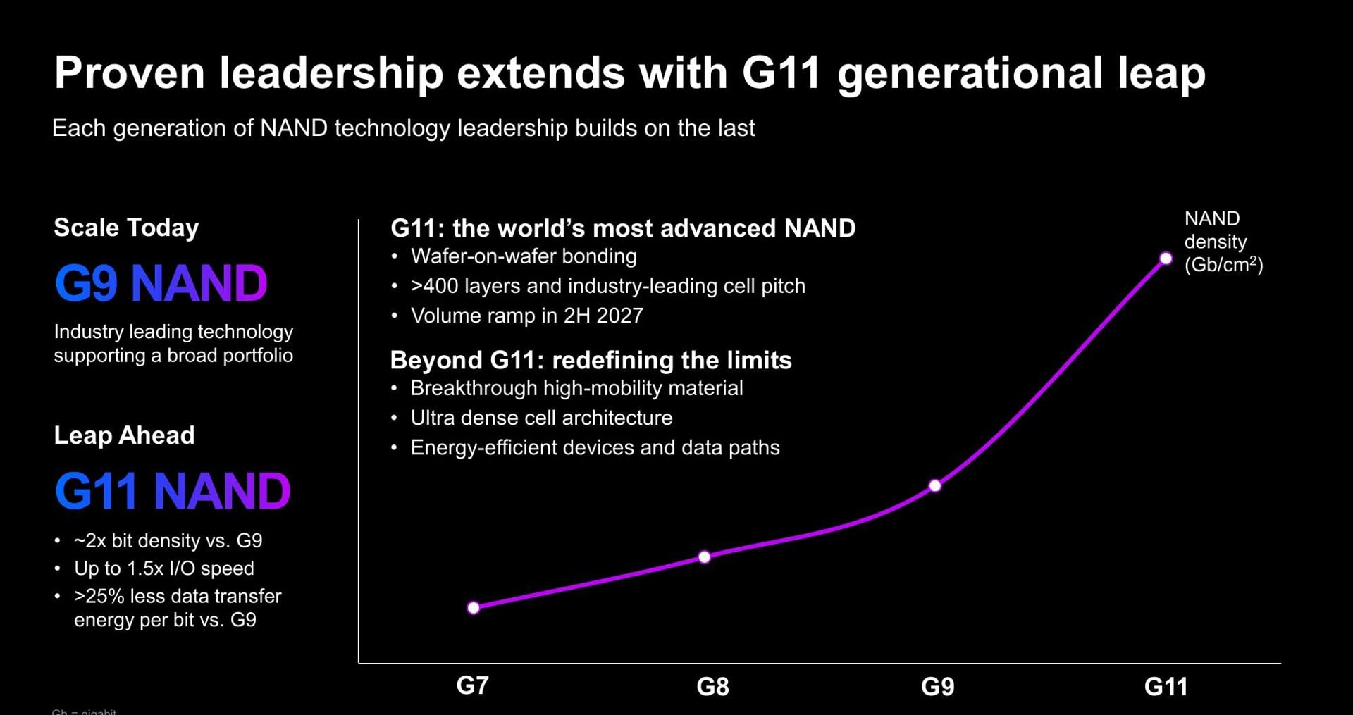
“We’ve actually gone back and ensured that this memory is optimized for the AI products of the future, and intentionally, which is why it goes from Gen 9 to Gen 11,” DeBoer said. “We’ve made substantial improvements that this node really brings relative to any prior NAND.” The slide labels G9 as “Scale Today” and G11 as “Leap Ahead,” with a “Beyond G11” list of a high-mobility channel material, an ultra-dense cell architecture, and energy-efficient data paths. On layers, DeBoer said, “We’ll be at more than 400 layers, and we’ll give more specifics on that next year, closer to the launch dates.”
What Wafer-on-Wafer Bonding Changes
DeBoer said Micron had held the technique back on purpose: “We’ll bring in wafer-on-wafer bonding technology at the right time when it’s cost effective and it brings in capability that’s important for the product specs at the time. And this is the right timing for that technology.”
He did not describe the mechanism, so this is our interpretation. Current 3D NAND builds the peripheral CMOS and the memory array on one wafer, either beside the array or underneath it, and every added layer in the array stack makes the etch through it harder and the yield lower. Bonding a separately processed array wafer to a separately processed logic wafer breaks that coupling: each wafer gets its own process, and the stack height stops being limited by what the periphery can tolerate.
That is the path to 400-plus layers without the yield penalty of a taller monolithic stack, and it is the same direction the deck shows for DRAM, where wafer bonding sits on the 1-epsilon node after the 1-delta ramp in the second half of 2027. For NAND, the 2x density claim is per unit area, charted in gigabits per square centimeter, so it is a wafer-cost statement as much as a capacity one. The 1.5x I/O figure is against G9, which Micron rated at 3.6GB/s when it launched the node in the 2650 client SSD i juli 2024.
A 512TB Number From Micron
Two slides later, Micron puts a figure on where the density goes. Its future AI-optimized storage slide lists next-generation data center SSDs as “high-performance, high-capacity (up to 512TB),” alongside a high-IOPS class rated at 25 million to 100 million IOPS for small-block access. The 245TB Micron 6600 ION we reviewed in Juneoch priced against hard drives in September, is built on G9 QLC; doubling the bits per wafer is how the next capacity step fits in the same E3.L envelope.

The timing fits what Micron’s Bill Bollengier told us on the podcast the same day: the company is lining up E1.S, E3.S, E3.L, and E2 for the density PCIe Gen6 and Gen7 platforms will want, with a 16K indirection unit to hold DRAM requirements down as capacities climb. The 512TB figure is a roadmap label, not a product, and Micron attached no date, interface, or cell type to it. DapuStor showed a 512TB QLC drive at FMS in August, so the number is already on the show floor; the G11 ramp is what makes it a volume part.
Two Kinds of AI-Class NAND
The deck splits a new category Micron calls AI-class NAND into two designs. The first is high-IOPS NAND, which DeBoer described as “SLC-based designs implemented in small blocks to design ultra-fast memory storage products” and called “a major focus for Micron in terms of getting these products out to market over the next couple years”; the targets are GPU-initiated small-block access for vector search, graph analytics, and AI context, and the deck’s 25M to 100M IOPS tier. The second is high-bandwidth NAND: TSV-stacked dies on a logic base die, forming a high-capacity tier close to the accelerator for model weights, long context, and KV cache.
The second design is a flash stack with an HBM-style base die, and DeBoer was specific about where it doesn’t fit: along the shoreline of the GPU, where HBM sits, because “we don’t think that has merit.” It belongs, in his words, “along closer positioning points to the compute itself.” He also said these parts “are more costly and have to be implemented in partnership with customers” to hit the cost point that makes them worth building. Micron has not named a product, a bandwidth figure, or a customer for either design.
Why the Ramp Date Matters
The second half of 2027 is also the window Micron has told investors to watch for supply. On its fiscal fourth quarter call on September 30, CEO Sanjay Mehrotra said, “We expect memory and storage supply-demand conditions to be much tighter in calendar 2027 and 2028 than they were in 2026,” and that the company does “not have line of sight to when supply and demand will return to balance.” He put industry NAND bit growth in the low-20s percent range this year and the mid-20s next year, with the industry supply constrained in both.
Asked on the webinar about rack-scale compute, DeBoer repeated the point: “We don’t see a period of time where memory is not going to be in short supply in the next two years, as Sanjay said, and we actually don’t see a time when it comes into balance.”
Micron’s own NAND supply grows more slowly than the industry’s this calendar year, and G9 is, with 1-gamma DRAM, its largest production node. Data center SSD revenue in the quarter was nearly $10 billion, more than ten times the year-ago figure and two-thirds of Micron’s NAND business. Against that backdrop, a node that doubles bits per wafer in 2H 2027 is the first new density lever inside the shortage Micron describes, and it arrives in the same half as the 1-delta DRAM ramp and the 512 GB DDR5 RDIMM volume production the company announced in September.



 Amazon