

AMD announced that its Spartan UltraScale+ SU200P FPGA will enter volume production in July 2026. The SU200P is the largest device in the Spartan UltraScale+ family. It expands AMD’s cost-optimized FPGA portfolio with a combination of high I/O density, low power operation, flexible connectivity, and integrated security features designed for long-lifecycle deployments.
Built on a 16nm FinFET process, the SU200P packs 218,000 system logic cells, 6.8Mb of block RAM, and 18Mb of UltraRAM, up to eight 16.3 Gb/s GTH transceivers, PCIe Gen4 x8 hard IP, and LPDDR4X/LPDDR5/LPDDR5X memory controllers running up to 4,266 Mb/s. AMD targets the device at applications spanning data center infrastructure, networking equipment, industrial automation, and embedded systems, where programmable control, connectivity, and security are increasingly critical.
Scalable FPGA Platform
The SU200P sits at the top of the nine-device Spartan UltraScale+ family and is designed to simplify migration across performance tiers. AMD emphasizes footprint compatibility across the product family, including between the SU65P and SU200P devices, allowing customers to reuse board designs as requirements evolve.
| Capability | SU200P FPGA |
|---|---|
| System logic cells | 218,000 |
| 1.0V – 3.3V I/O | Up to 572, 3.2 Gb/s MIPI |
| Block RAM / UltraRAM | 6.8 Mb / 18.0 Mb |
| GTH transceivers | Up to 8 × 16.3 Gb/s |
| PCIe hard IP | Gen4 x8 |
| Hard memory controllers | LPDDR4X / LPDDR5 / LPDDR5X up to 4,266 Mb/s |
| Lifecycle | 2045 |
The SBVF900 package also aligns with the Kintex UltraScale+ Gen 2 family, providing a migration path to higher-performance FPGAs without requiring a board redesign. This compatibility can help reduce engineering effort and preserve hardware investments across multiple product generations.
Security Designed for Long-Lifecycle Systems
Security is a major focus of the SU200P, particularly for systems expected to remain deployed for years in environments such as data centers, industrial facilities, and medical infrastructure.
The device incorporates a hardware root of trust and support for post-quantum cryptography aligned with CNSA 2.0 requirements. AMD says the platform is designed to protect device identity, secure firmware authentication, and support trusted updates throughout the operational lifecycle.

Security features include hardware root of trust secure boot, AES-GCM authenticated encryption, dedicated cryptographic engines, a true random number generator compliant with NIST and AIS standards, and a physical unclonable function (PUF) for device-specific identity and key protection. Together, these capabilities establish a chain of trust from manufacturing through field deployment and ongoing firmware maintenance.
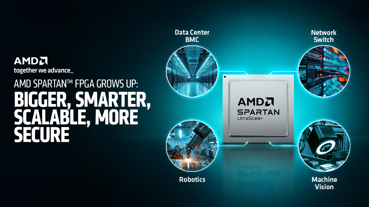
Targeting Data Center Infrastructure
AMD positions the SU200P as a companion FPGA for increasingly complex server platforms. Modern servers continue to add sensors, telemetry sources, power domains, and management interfaces, while the growth of AI infrastructure is driving demand for more sophisticated board-level control functions.
The company highlights the FPGA’s potential role as a platform root of trust, enabling device attestation and secure boot capabilities before host processors initialize. The device supports up to 572 I/O pins, PCIe Gen4 connectivity, 3.3V I/O, and programmable control logic that adapts to evolving server architectures and management standards.
AMD also notes support for emerging Open Compute Project technologies such as the Low-speed Transport Protocol Interface (LTPI) and the Management Port Embedded Secure Tunnel Interface (M-PESTI), which are becoming increasingly relevant in next-generation server designs.
Consolidating Functions in Network Switches
For networking applications, the SU200P is designed to integrate control-plane management, interface adaptation, monitoring, and security functions into a single programmable platform.
The FPGA includes PCIe Gen4 connectivity, GTH transceivers, up to two hard memory controllers, and support for the AMD MicroBlaze V soft processor running a real-time operating system. This allows switch vendors to consolidate management and control functions while reducing component count and board complexity.
Security capabilities are integrated into the device’s configuration architecture, enabling secure boot, authenticated firmware updates, hardware-based device authentication, and post-quantum cryptography support throughout the product lifecycle.
Industrial Focus with Extended Availability
Industrial automation, robotics, edge control systems, and sensor aggregation platforms are other key target markets for the SU200P.
AMD has committed to supporting the device through at least 2045, addressing a common requirement in industrial markets where systems often remain deployed for decades. The FPGA integrates up to 18Mb of UltraRAM, GTH transceivers, hard memory controllers, and high I/O density, enabling designers to reduce external components, board area, power consumption, and overall system complexity.
Combined with its integrated security architecture, the device is intended to support long-term deployments that require secure firmware management and a protected device identity over extended operating lifecycles.
Availability
The AMD Spartan UltraScale+ SU200P FPGA enters volume production in July 2026. AMD positions the device as a scalable platform for customers requiring a balance of programmable logic, connectivity, security, and long-term availability across data center, networking, and industrial deployments.


 Amazon