

At its Advancing AI event in San Jose, AMD unveiled the Instinct MI350 series, its latest generation of GPUs, alongside an aggressive roadmap for future AI accelerator platforms. Built on the advanced CDNA4 architecture, the MI350 series promises substantial performance uplifts for demanding AI workloads. This announcement also included a preview of the future Instinct lineup, underscoring AMD’s commitment to continuous innovation in AI hardware.
AMD Instinct MI350 Series
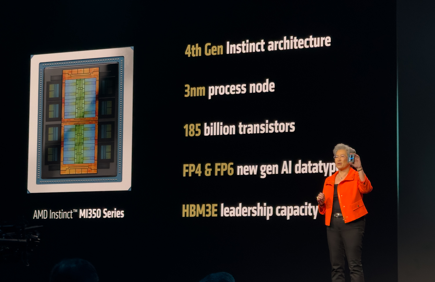
The AMD Instinct MI350 series, powered by the new CDNA4 architecture, represents a significant leap forward in AI computation. Specifically designed for AI workloads, the CDNA4 architecture introduces enhanced matrix engines, support for new data formats, and critical improvements in energy efficiency.
Advanced Packaging and Chiplet Architecture: The Foundation of MI350
The MI350 series is built upon AMD’s advanced 3D chiplet packaging technology, evolving from the MI300 series with key enhancements.
Chiplet Design and Fabrication
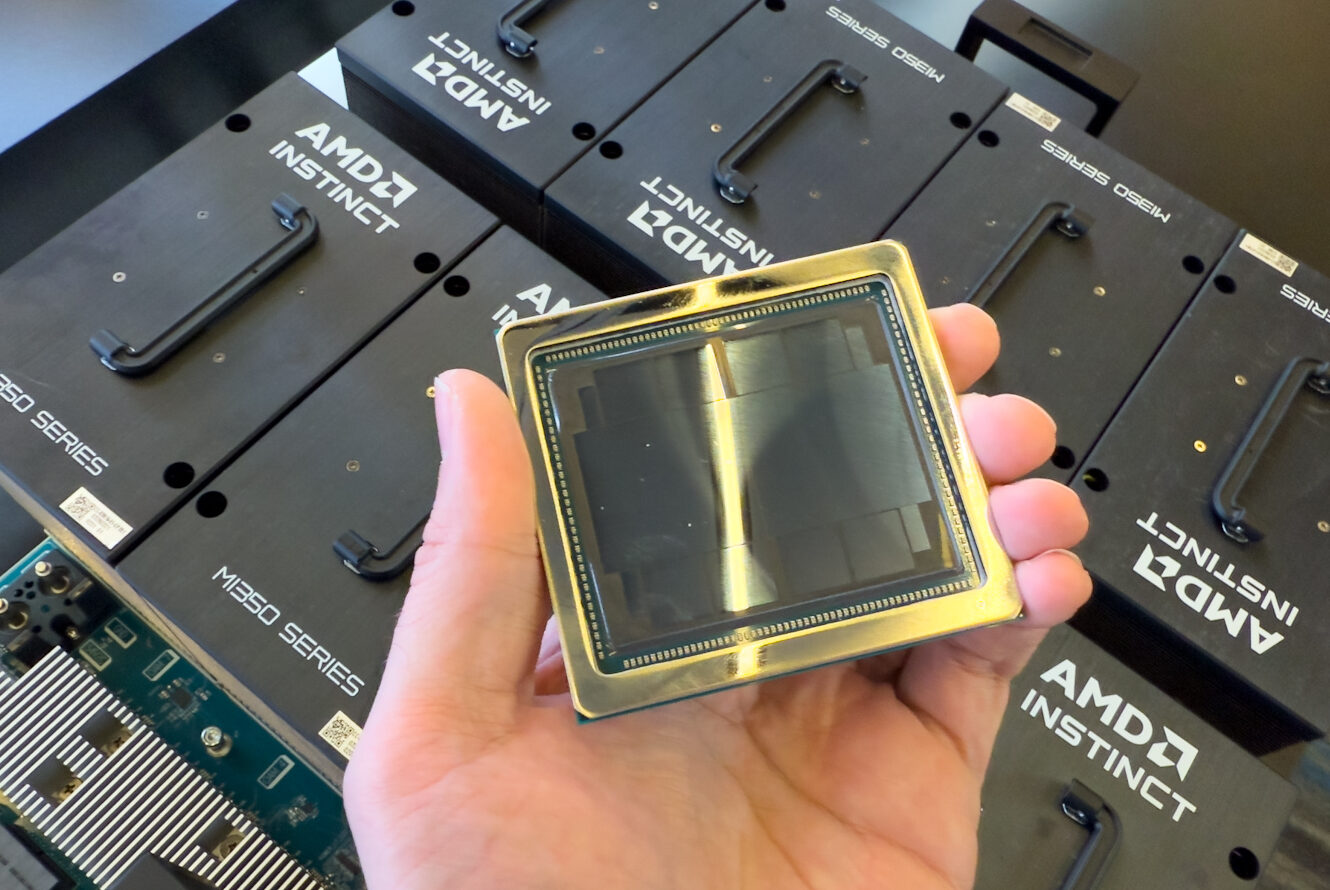
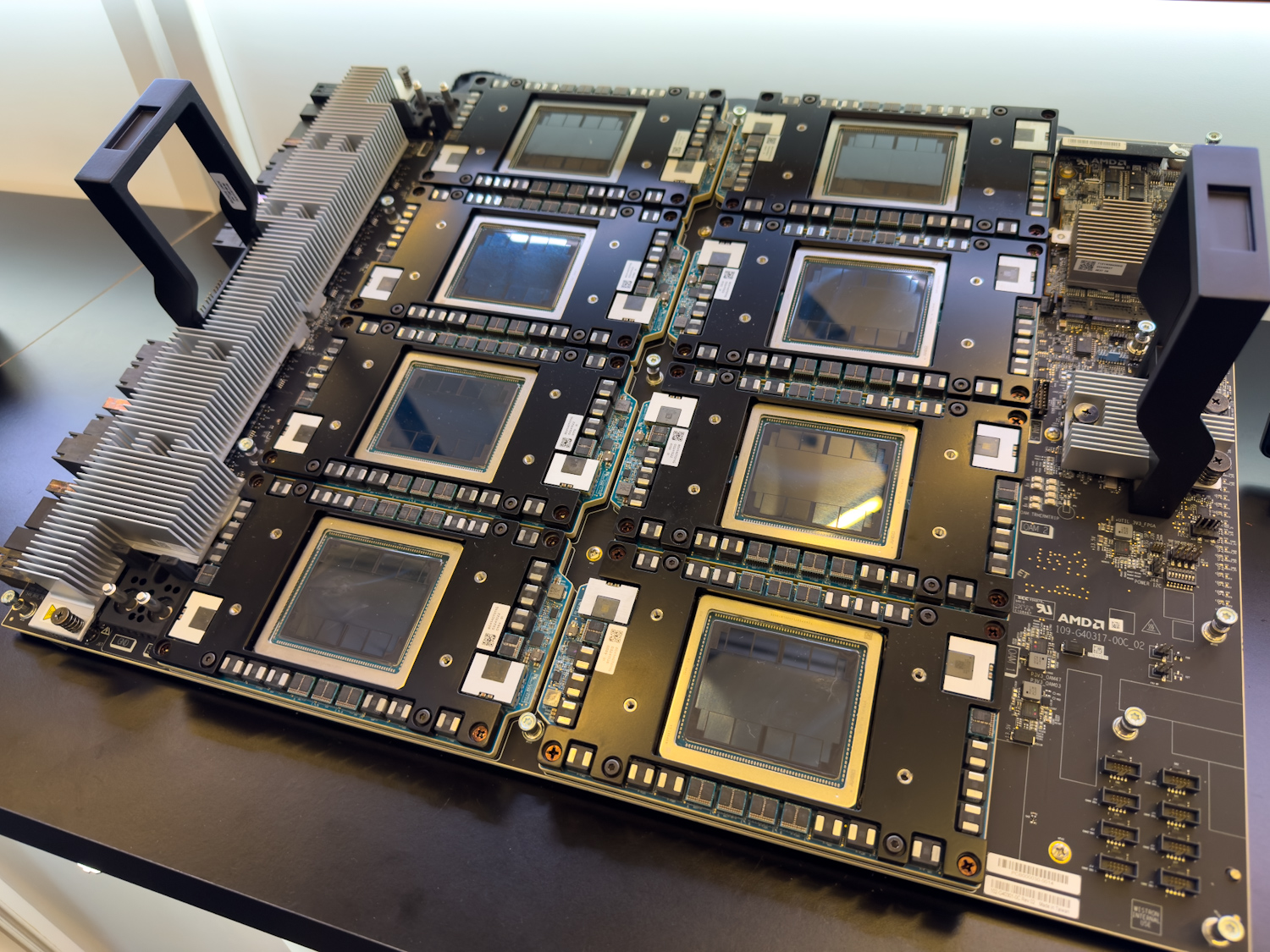
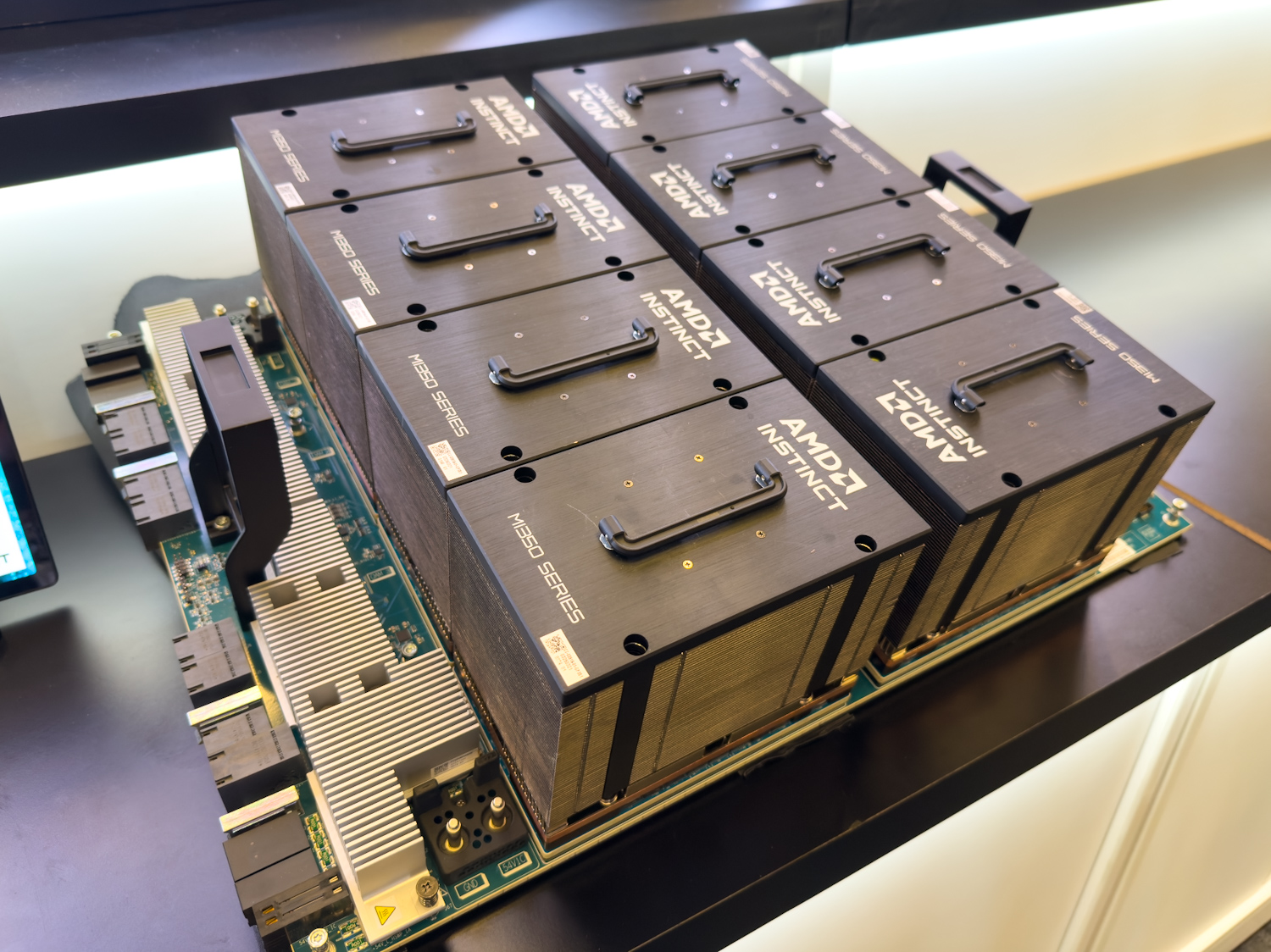
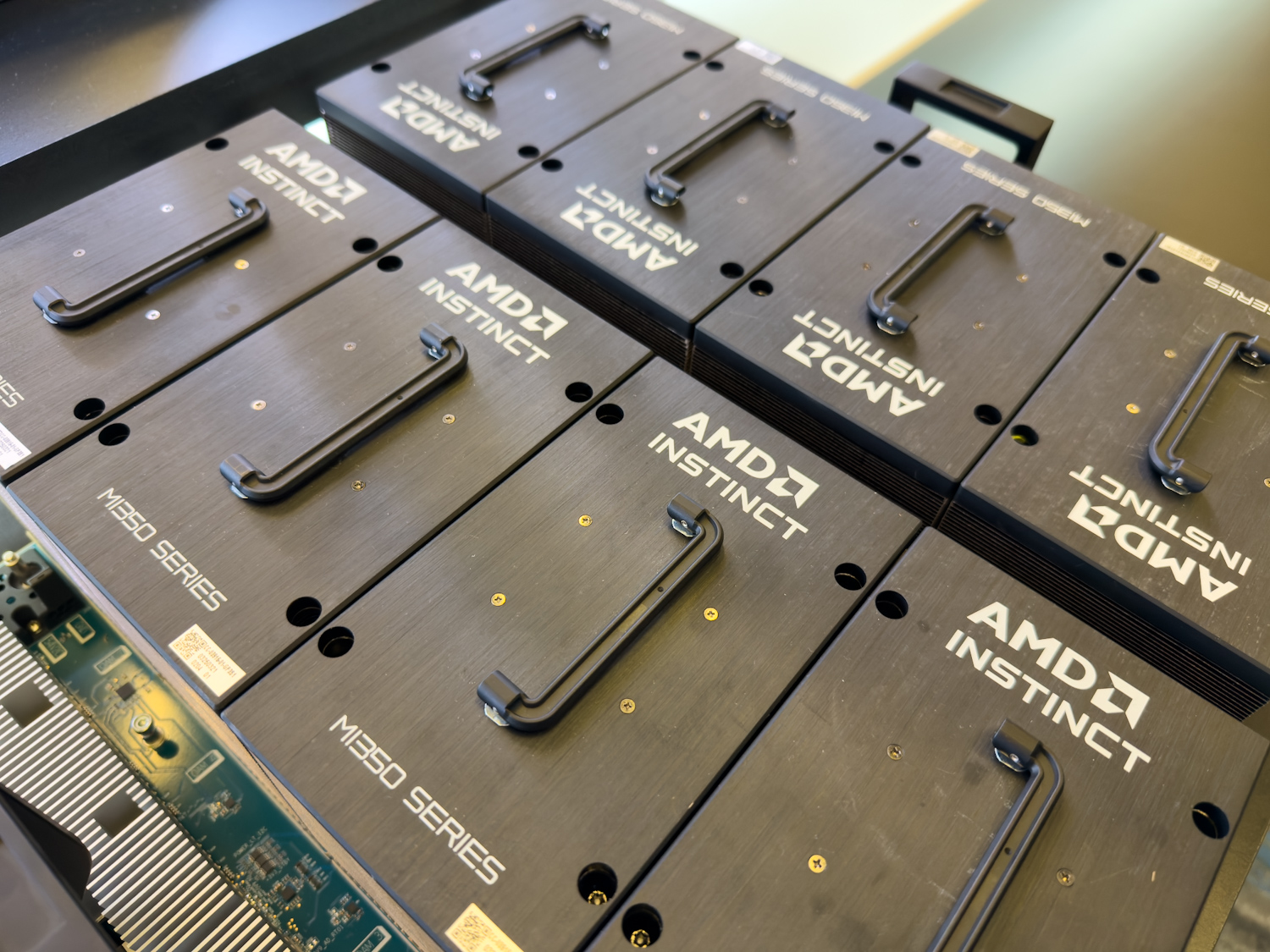
At its core, the GPU package features eight Accelerator Compute Chiplets (XCDs), the primary computational engines. These XCDs are fabricated on an advanced 3nm Node 3+ node process, an upgrade from the 5nm technology used in the MI300 series, contributing significantly to improved energy efficiency. Each XCD houses four shader engines, with each engine containing eight active CDNA4 compute units, culminating in 32 CUs per XCD and a total of 256 CUs for the accelerator.

Complementing the XCDs are two IO Dies (IODs), a reduction from the four IODs in the MI300 series. These IODs, manufactured on a 6nm-class process, handle memory access, I/O operations, and inter-chiplet communication. This streamlined two-IOD design, combined with wider internal interconnects, maintains bandwidth targets while reducing power consumption.
Physical Integration and Logical Unity
The physical assembly involves mounting the XCDs and HBM3E memory stacks on a Chip-on-Wafer-on-Substrate (COOS) interposer. A critical aspect of this design is the hybrid bonding of XCDs to the IODs situated beneath them. This 3D hybrid bonding technique creates exceptionally dense, high-bandwidth interconnects between the compute and I/O chiplets, far exceeding traditional 2.5D constructions, which is vital for efficiently supplying data to the power-hungry XCDs. Furthermore, this advanced 3D integration contributes to a smaller overall GPU footprint, which may enhance manufacturing yield and operational reliability.
Despite its complex chiplet construction, the MI350 logically functions as a single, unified GPU. Each XCD constitutes an Accelerator Compute Complex, equipped with global resources, including a command processor and a 4MB L2 cache.
Enhanced Memory Subsystem
To adequately supply the powerful CDNA4 cores, the MI350 series features a substantially upgraded memory subsystem. It is equipped with eight stacks of HBM3E memory, providing a total capacity of 288GB per GPU. Each 36 GB stack, composed of 12-high 24Gbit devices, operates at the full HBM3E pin speed of 8Gbps per pin.
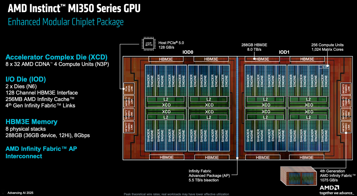
The architecture also retains AMD’s Infinity Cache, a crucial memory-side cache positioned between the HBM and the Infinity Fabric/L2 caches. This cache comprises 128 channels, each backed by 2MB of cache, for a total of 256MB for the GPU. To enhance bandwidth delivery efficiency at lower power, AMD has widened the on-die network buses within the IODs and operates them at a reduced voltage. This optimization reduces the energy per bit, enabling the MI350 series to achieve approximately 1.3 times higher memory bandwidth per watt compared to its predecessor, the MI300 series.
Furthermore, to effectively manage the expansive 288GB physical memory, the Universal Translation Caches (UTCs) analogous to CPU Translation Lookaside Buffers (TLBs) have been significantly enhanced. The MI350 series introduces more granular page size controls in both UTC L1 and L2, alongside increased capacities. These improvements allow for a greater TLB reach and more efficient virtual memory management.
Infinity Fabric Enhancements
AMD’s Infinity Fabric technology remains central to the MI350’s scalability and inter-GPU communication performance. The bisectional bandwidth of the Infinity Fabric AP link connecting the two IODs has been substantially increased to 5.5TB/s, facilitating efficient data movement between the GPU’s two halves.
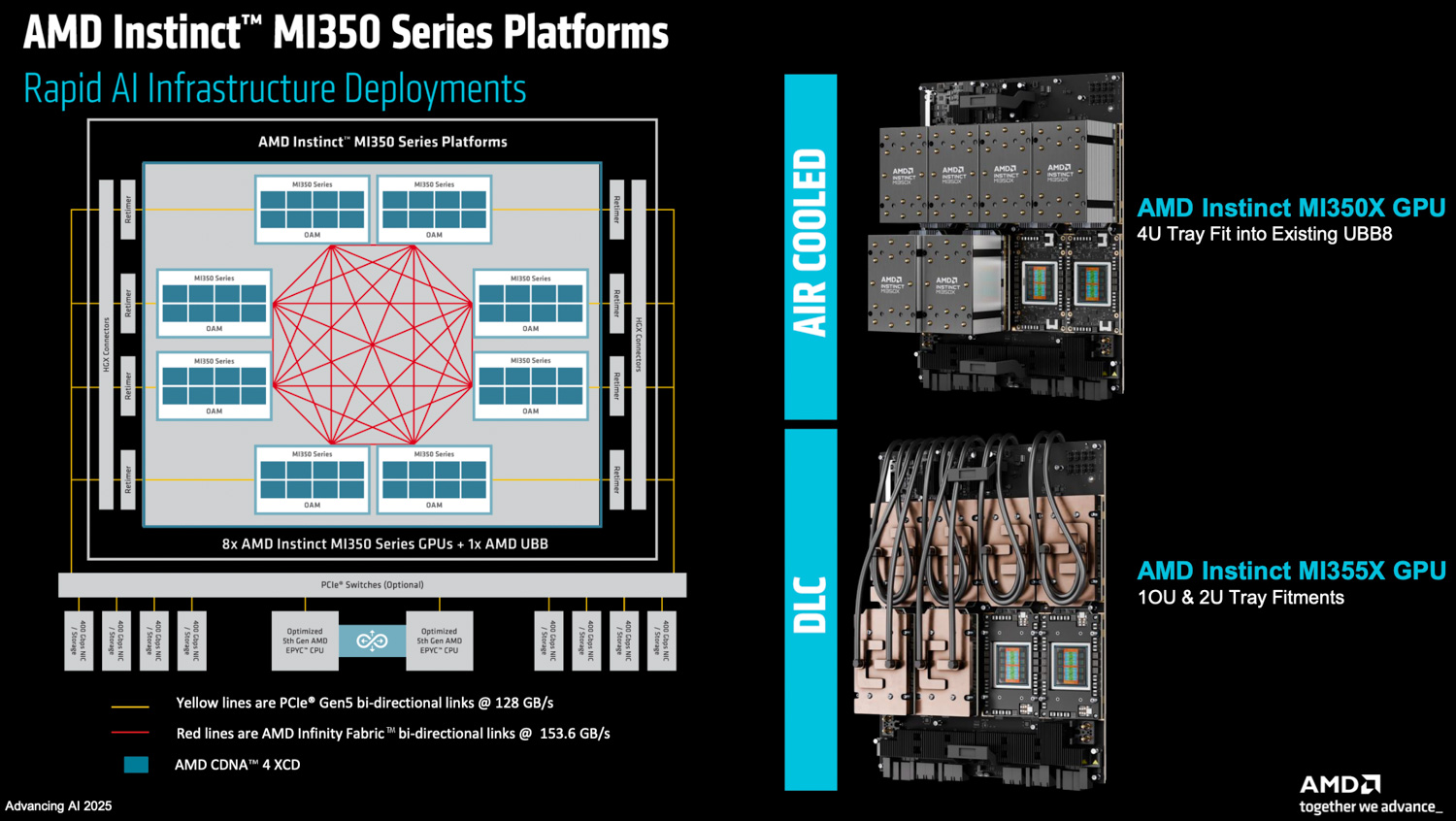
For external communication, each MI350 GPU features seven Infinity Fabric links, enabling direct GPU-to-GPU connectivity in configurations such as an 8-GPU UBB 2.0 platform. These links operate at 38.4Gbps per pin. In an 8-GPU OAM setup, this configuration delivers a bisectional bandwidth of approximately 153.6 GB/s in each direction per link. AMD has also refined data packing and compression techniques over these external links to boost the effective delivered bandwidth. Internally, the Infinity Fabric ensures that all XCDs have full, fine-grained interleaved access to the entire HBM3E memory space across both IODs, presenting the memory as a single, flat, unified resource to the compute units.
CDNA4 Compute Core Architecture
At the heart of the MI350’s processing power, the CDNA4 compute unit, has undergone a significant re-architecture tailored for AI.
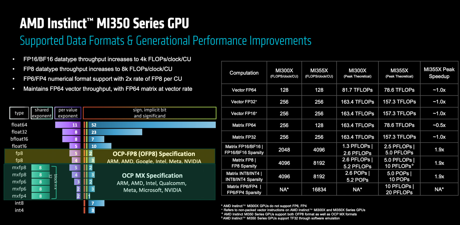
Matrix math capabilities see a substantial boost: MI350 CUs deliver a 2x increase in throughput per CU for 16-bit (BF16, FP16) and 8-bit (FP8, INT8) operations compared to their MI300 counterparts. The MI350 series also introduces hardware support for OCP MX-specified micro-scale formats, specifically FP6 and FP4, which scale proportionally from FP8. Notably, AMD’s implementation enables FP6 to operate at the same computational rate as FP4. This strategic decision positions AMD for leadership in FP6, an emerging format with potential for AI training. Furthermore, a new vector ALU has been added, supporting 2-bit operations and capable of accumulating BF16 results into FP32, thereby enhancing throughput for certain low-precision vector operations.
To support these enhanced tensor throughputs, the Local Data Share (LDS) size per CU has been increased, and new capabilities enhance bandwidth for loading data from global memory into the LDS. Recognizing potential bottlenecks in operations like softmax and attention mechanisms, the throughput for transcendental functions has also been increased in tandem with the tensor core improvements.
Several other architectural enhancements contribute to performance and flexibility:
- Hardware-Supported Stochastic Rounding: Mitigates bias when downcasting from FP32 to lower precision formats by injecting entropy.
- Logical Operator 3 (LUT3) Instruction: Offers programmers greater flexibility for implementing custom three-input logical operations.
- New Min-Max Operators: Enable programmers to control NaN propagation during comparisons, allowing them to either propagate NaN values or select the non-NaN floating-point number, thereby aiding in robust AI data management.
While AI is the primary focus, the MI350 series retains support for 64-bit floating-point (FP64) operations in both vector and matrix units. However, a key difference from the MI300 is that on the MI350, matrix FP64 operations run at the same rate as the vector FP64 units, effectively half the FP64 matrix rate of the MI300.
Finally, the combination of higher HBM3E bandwidth and a slightly reduced CU count (256 on MI350X/355X versus 304 on MI300X) means each CU in the MI350 series benefits from increased global memory bandwidth per clock. This is crucial for accelerating both GEMM-heavy (General Matrix Multiply) operations and bandwidth-bound vector arithmetic.
Partitioning for Flexibility: NPS and Compute Partitioning
The AMD MI350 series features enhanced partitioning capabilities, offering highly flexible allocation of its substantial resources to maximize utilization and efficiency across diverse workloads.
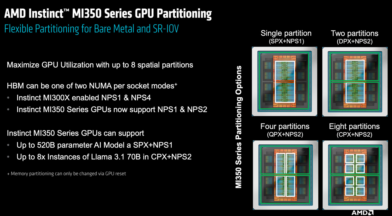
For memory management, the MI350 provides two primary NUMA (Non-Uniform Memory Access) modes:
- NPS1: Treats the entire 288GB HBM3E memory as a single, unified NUMA domain by interleaving data access across all eight HBM stacks.
- NPS2: Divides the memory into two separate NUMA domains, each corresponding to one of the two IODs and its four associated HBM stacks. While memory access within each IOD in NPS2 mode remains fine-grained interleaved, it becomes coarse-grained across the IODs. This mode, particularly when combined with compute partitioning, can enable optimizations for spatial locality.
Notably, AMD has opted not to support an NPS4 mode on the MI350 (which was available on the MI300). The decision stems from the tighter memory coupling within each of the two IODs on the newer architecture, which diminished the potential performance benefits of further memory subdivision.
On the compute side, the GPU can be configured to operate in several modes:
- SPX (Single Partition Execution): The GPU operates as a single, powerful engine, typically used with NPS1 memory mode.
- DPX, QPX, OPX (Dual, Quad, Octal Partition Execution): The GPU can be divided into two, four, or even eight independent compute partitions, respectively.
These compute partitions can be paired with either NPS1 or NPS2 memory configurations, with the constraint that the compute partition’s granularity must be at least as fine as, or finer than, the memory partition (e.g., SPX mode is incompatible with NPS2 memory partitioning).
These versatile partitioning options are supported in both bare-metal deployments and through SR-IOV (Single Root I/O Virtualization), making them ideal for virtualized, multi-tenant environments. For instance, in cloud or data center settings, a single MI350 GPU can be logically segmented to serve multiple users or applications concurrently. Each tenant receives a dedicated slice of memory and compute resources, ensuring quality of service and security, which is particularly valuable for scenarios where different virtual machines require isolated access to GPU hardware.
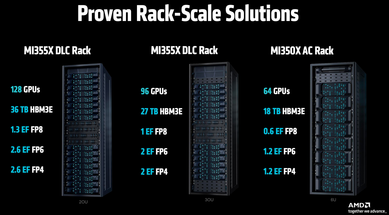
MI350X vs. MI355X: Tailored for Different Deployments
The MI350 series is introduced with two primary variants, catering to different deployment needs and thermal envelopes:
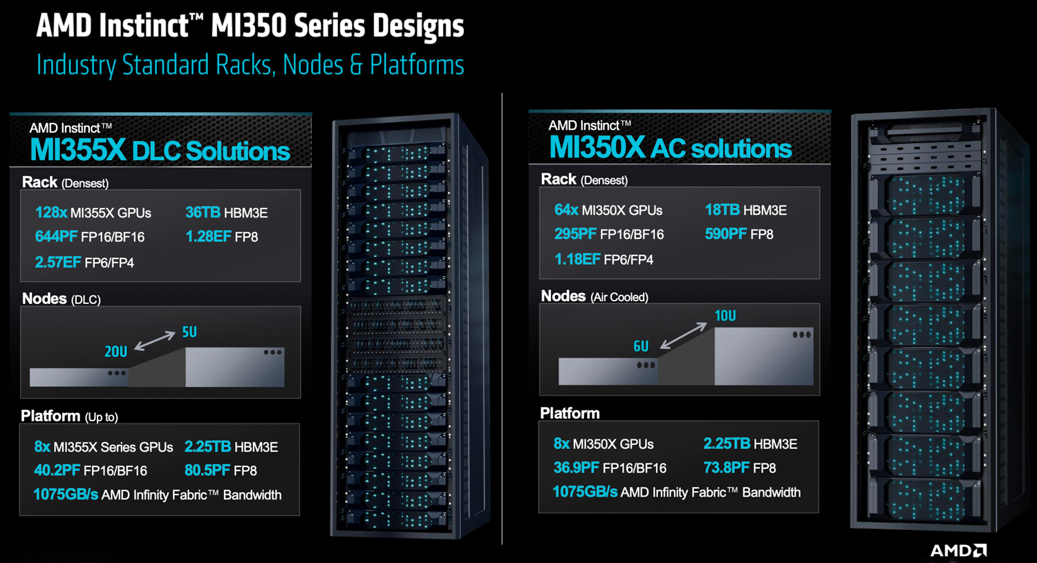
- MI350X: This variant is designed for lower power consumption, with a Thermal Design Power (TDP) of up to one kilowatt. It supports air-cooled deployments, offering broader compatibility within existing data center infrastructures.
- MI355X: Operating at a higher system power of up to 1.4 kilowatts TDP, the MI355X is primarily targeted towards liquid-cooled deployments, enabling it to deliver maximum performance.
While both variants are built on the same fundamental hardware, the MI355X’s higher operational power envelope allows for higher sustained clock frequencies. This translates to an approximate 20% performance advantage in real-world, end-to-end workloads when compared to the MI350X. These are available in three validated rack configurations.
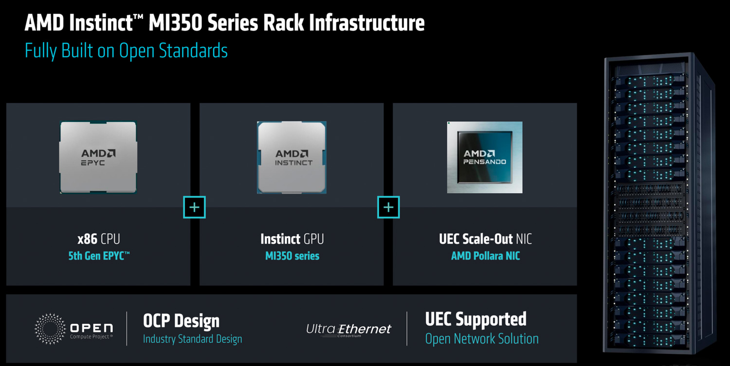
AMD Pensando Pollara Networking
In addition to the new GPUs, AMD provided an in-depth look at its Pollara Networking solutions, showcasing significant architectural advancements designed to meet the escalating demands of large-scale artificial intelligence systems. The Pollara 400 AI NIC, built upon technology from AMD’s Pensando acquisition, introduces a new level of programmability and intelligence to AI network fabrics.

The core of Pollara’s innovation lies in its programmable architecture. Unlike fixed-function hardware, the Pollara NIC features a P4-programmable MPU core. This design is crucial because AI networking requirements are in constant flux, with new protocols, transport mechanisms, and telemetry needs emerging rapidly. Programmability enables the Pollara NIC to adapt through software updates, allowing for the deployment of custom traffic management schemes, novel load balancing algorithms, and tailored congestion control mechanisms without requiring hardware replacement. This flexibility is crucial for future-proofing AI data centers and responding quickly to the evolving characteristics of workloads.
Addressing common network bottlenecks, Pollara introduces multicast. For GPU-to-GPU communication, data from a single connection can be distributed across multiple physical network links simultaneously. This approach enhances overall network utilization and throughput by preventing congestion on any single path. The NIC itself manages the complexities of this distribution, including the reordering of packets that may arrive at the destination out of sequence.
Network efficiency is enhanced through selective acknowledgment for retransmissions. In traditional networks, losing a single packet can trigger the retransmission of an extensive sequence of data. Pollara also implements a more precise method where only lost packets are resent. This significantly reduces redundant data on the network, improving effective bandwidth. The Pollara networking solution is also engineered for robust operation in diverse network environments, including those with lossy connections. It incorporates sophisticated, programmable, and path-aware congestion control. This capability reduces the reliance on perfectly lossless network fabrics, which can be complex and costly to implement and maintain at the massive scales required by modern AI clusters.

AMD is also an active participant in the Ultra Ethernet Consortium, contributing to and implementing its standards. UEC aims to define next-generation Ethernet optimized for AI, focusing on efficient load balancing, enhanced reliability, and AI-specific congestion control. Adherence to these open standards promotes interoperability and fosters a broader ecosystem.
Finally, the Pollara technology is designed for synergistic operation within AMD’s broader platform, enabling co-innovation across CPU, GPU, and NIC components. This includes capabilities like collective operation offload, where the NIC handles specific network-intensive communication tasks (those not requiring GPU computation). This frees up GPU resources for their primary processing tasks.
ROCm 7: An Open Software Ecosystem for Advanced AI
Underpinning these hardware innovations is the announcement of ROCm 7, the latest evolution of AMD’s open software platform, engineered to maximize performance and accessibility. Scheduled for a public preview today ahead of its full release in August, AMD reports ROCm 7 delivers a staggering 3x to 3.5x improvement in both inference and training performance on existing hardware compared to its predecessor.
For enterprise clients, AMD is launching ROCm AI Enterprise, a comprehensive suite offering cluster management, MLOps, and application-building tools for large-scale deployments. Simultaneously, AMD is enabling access for individual developers with a new developer cloud, complete with free GPU credits to encourage experimentation. This push for accessibility extends even further, with ROCm 7 officially expanding support to client devices, including laptops and workstations running Windows, ensuring developers can build and test AI applications seamlessly across the entire AMD ecosystem.
The Road Ahead
AMD is dedicated to a rapid, yearly cycle of innovation, with a product roadmap that extends beyond its MI350 series.

Looking ahead to a target launch in 2026, AMD is developing the MI400 series, which will be the core of a fully integrated, rack-scale solution codenamed Helios. This platform is being specifically engineered to train cutting-edge AI models and manage large-scale distributed inference tasks. The Helios system will be an integrated AMD platform, incorporating future EPYC CPUs codenamed Venice, Instinct MI400 GPUs, and next-generation Pensando networking, specifically the Vulcano 800G AI NIC. A comprehensive ROCm software stack, including a dedicated Fabric Manager for automated deployment and management, will also be part of this solution. Emphasizing open standards, the Helios rack will comply with OCP specifications. It will leverage Ultra Ethernet (UEC) for scaling out networking between racks and introduce the Ultra Accelerator Link (UAL 1.0) for scaling up communication within a single rack.

The Instinct MI400 GPU itself is purpose-built for extreme-scale AI applications. Preliminary specifications indicate impressive capabilities, including 40 PetaFLOPS of FP4 performance and 20 PetaFLOPS of FP8 performance. Each GPU is expected to feature 432 gigabytes of HBM memory, delivering approximately 20TB/s of HBM memory bandwidth, and will offer 300 Gigabits per Second of scale-out bandwidth. Complementing the GPU, the Vulcano 800G AI NIC will be UEC-ready and support UAL alongside PCIe Gen6, with UAL providing twice the bandwidth of PCIe Gen6. This NIC is anticipated to offer up to eight times more scale-out bandwidth per GPU compared to the earlier Polara generation. AMD has ambitious performance goals for the Helios rack solution, projecting it to deliver up to ten times more AI performance on the most advanced frontier models when compared to the MI355. Against Vera Rubin in 2026, Helios aims to offer competitive raw FLOPS, 50% more HBM capacity, 50% more HBM memory bandwidth, and up to 50% more scale-out bandwidth.
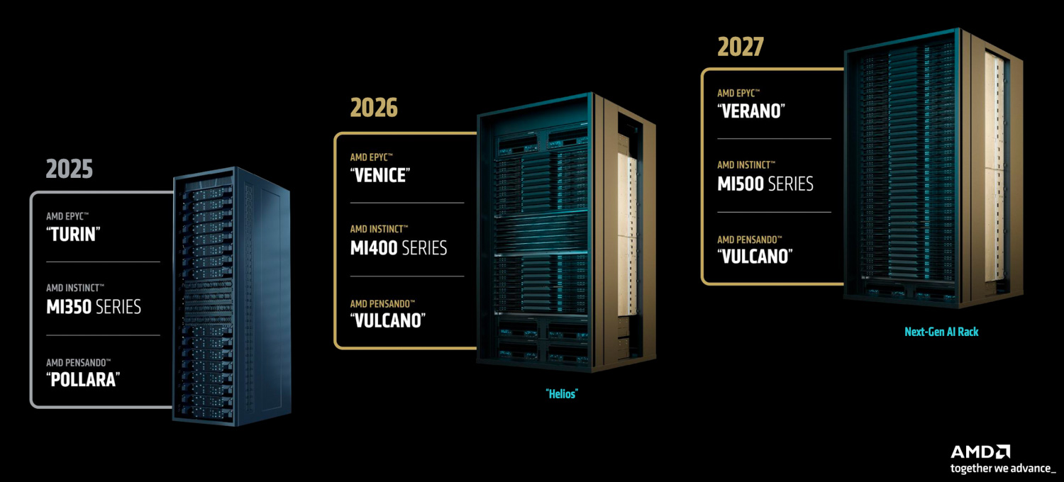
AMD’s roadmap extends even further, with development already well underway for the MI500 series and subsequent rack-scale architectures planned for 2027 and beyond. These future platforms will integrate the MI500 series, alongside next-generation EPYC CPUs codenamed Verano, and further advancements in Pensando networking technology. Additional information, however, was not disclosed at the event.


 Amazon