

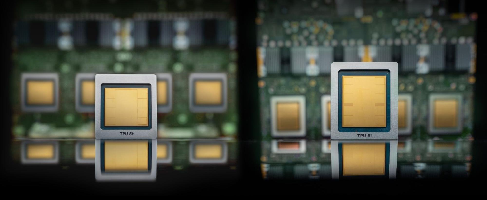
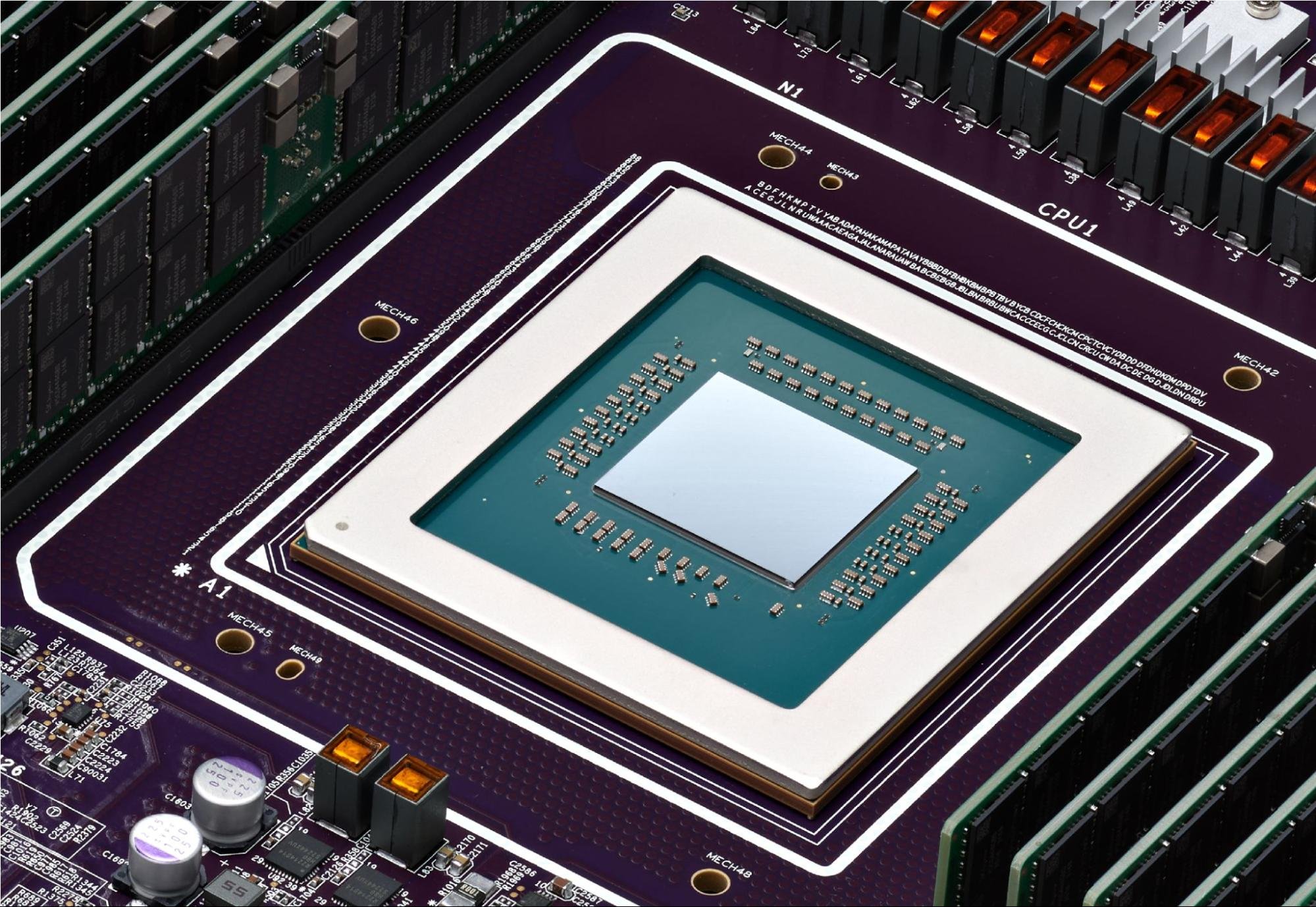
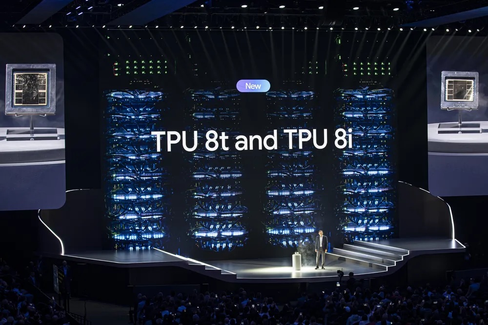
At Google Cloud Next, Google announced its next-generation AI accelerators: the TPU 8t “Sunfish” for training and the TPU 8i “Zebrafish” for inference, along with its new Virgo data center fabric. From Google’s blog posts, it is clear these chips are optimized for “the agentic era”: training frontier mixture-of-experts models at the hundreds-of-thousands-of-chips scale, and then serving those same models at low latency and aggressive price-per-token targets. The 8t and 8i are two architecturally distinct chips that share a host platform and a fabric but diverge on memory capacity, on-chip SRAM, interconnect topology, and on-die specialization. The 8t is built for dense matrix multiplication (matmul) at scale, while the 8i is built around KV cache on silicon and per-token collective latency.
A single 8t superpod scales to 9,600 chips, holds 2 PB of HBM, and delivers 121 EFLOPS of FP4 compute, nearly 3x the per-pod compute of an Ironwood superpod. 8i pairs 288 GB of HBM with 384 MB of on-chip SRAM (3x Ironwood) within a 1,152-chip scale-up domain and claims 80% better performance-per-dollar than Ironwood for LLM inference. Virgo binds both chip families into a single data center fabric that links more than 134,000 8t chips at 47 Pb/s of non-blocking bisection bandwidth, with up to 4x the per-accelerator bandwidth and 40% lower unloaded latency than the prior generation.
What a TPU Actually Is
Before getting into the 8 silicon, some background on what a TPU is and how it differs from a GPU, because the 8 design decisions only make sense against that context.
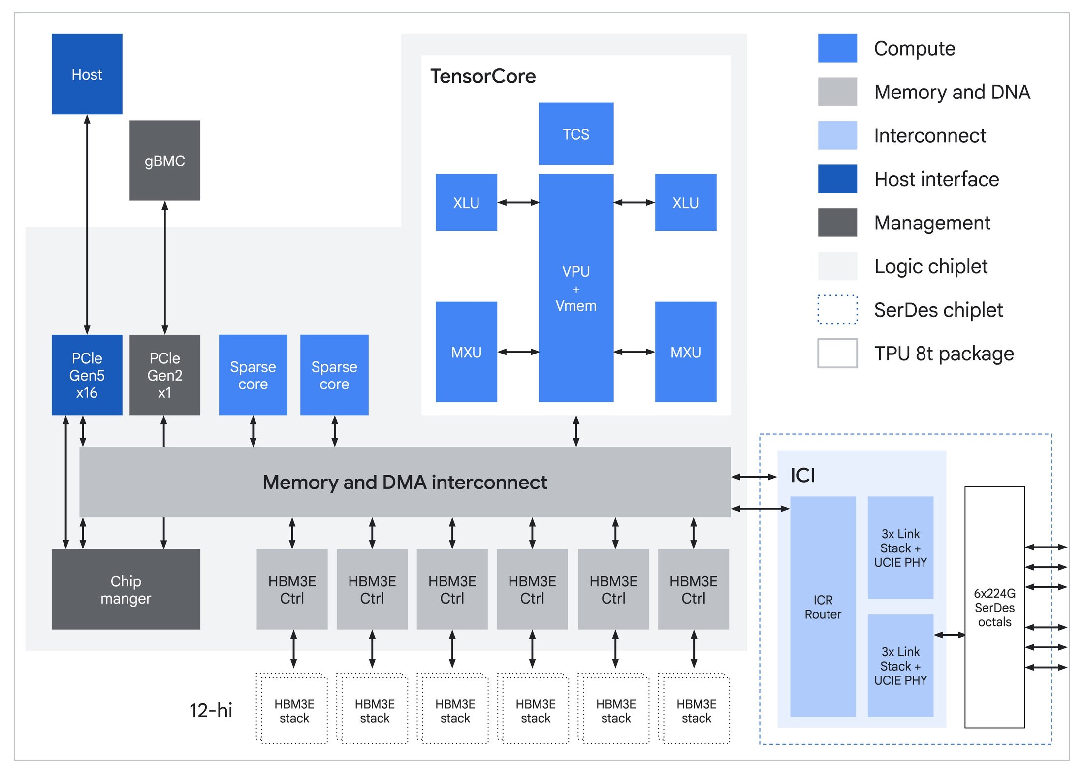
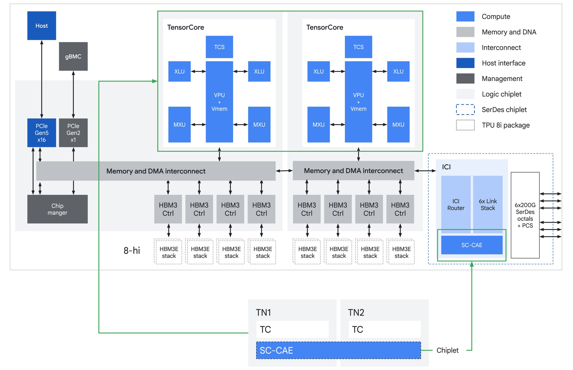
A Tensor Processing Unit is a custom ASIC that Google has been iterating on since 2015. Every generation has been built around the same core idea: instead of scheduling thousands of small cores dynamically, as a GPU does, a TPU centers on a small number of very large MXUs (matrix multiply units), fed by an on-chip, software-managed SRAM scratchpad, and driven by an ahead-of-time compiler. Each chip carries a handful of TensorCores, each built around one large systolic-array MXU, plus a smaller set of SparseCores dedicated to the irregular gather-scatter lookups that dominate recommendation embeddings. Data flows from HBM through the scratchpad, through the MXU, back to the scratchpad, and out again, with a Vector Processing Unit handling activations, normalizations, and reductions alongside. There is no hardware warp scheduler, no L1 or L2 cache hierarchy in the GPU sense, and no dynamic dispatch.
The upside of this design is efficiency in dense linear algebra. With an ahead-of-time compiler deciding where every tensor lives and when every collective fires, there is no cache-miss jitter and no warp-scheduler tax, which matters more than it sounds when tens of thousands of chips have to stay synchronized through a collective. Real-world model FLOP utilization on TPUs for well-tuned training workloads tends to be higher than on traditional GPUs. The downside is that anything that does not map cleanly to large dense matmuls, specifically dynamic shapes, irregular sparsity patterns, MoE routing with uneven token distribution, or graph neural networks, is harder to express efficiently. TPUs have also historically carried less HBM per chip than their GPU counterparts and have had much narrower framework support. XLA and JAX are first-class; PyTorch has, until recently, required a translation layer; in addition, the compiler, runtime, networking libraries, and multi-pod software stack remain closed-source within Google.
Sparsity is the cleanest example of the philosophical gap between GPUs and TPUs, and the reason is structural rather than marketing. NVIDIA has supported 2:4 structured sparsity on Tensor Cores since Ampere, and, on paper, performance for sparse workloads is double that of dense workloads. A Tensor Core is fundamentally a dispatch unit: it takes explicit operand loads per MMA instruction, so adding a sparse MMA variant that accepts a compressed 2-out-of-4 block plus index metadata is a straightforward extension of the existing instruction set. Each cycle, the hardware pulls only the non-zero values and their indices into the multiplier array, implicitly skipping the zeros.
A systolic array works the opposite way. Every PE (processing element) computes every cycle, with operands streaming through the array in lockstep via direct register-to-register paths from one PE to the next. That deterministic dataflow is exactly where the power-efficiency advantage over SIMT comes from: no repeated SRAM reads, no instruction dispatch overhead, maximum operand reuse. But it also means the hardware cannot skip a zero-valued element per cycle without breaking the pipeline.

Source: Google
TPUs can still exploit sparsity at the tile level; if an entire MXU-sized tile is all zeros, the compiler does not schedule work on it. However, Google’s choice not to add hardware acceleration for structured sparsity is deliberate. Adding M:N structured sparsity to a systolic array can be achieved using multiple techniques, each with different trade-offs. One such technique requires a compression unit sitting between SRAM and the array’s input ports. But a systolic array is a pipeline, not a dispatcher. Its efficiency guarantee comes from operands arriving in a deterministic cadence, with every processing element busy every cycle. Allowing operands to be skipped forces one of two costs. Stall the pipeline on the zeros, which erases the efficiency advantage that motivated the architecture in the first place. Or add dedicated decompressor hardware to reconstruct a full-width stream from the compressed input before it enters the array, which would consume die area and add latency.
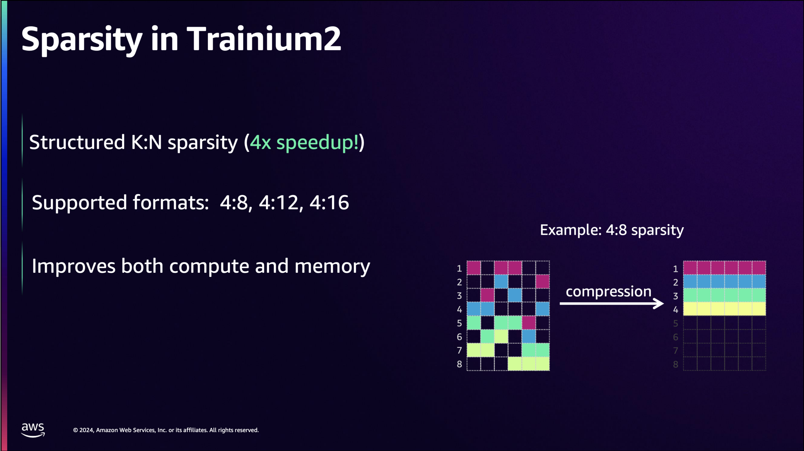
Source: AWS
Some accelerators pair systolic arrays with hardware support for sparsity. AWS built one starting with NeuronCore-v3, the engine inside Trainium2 and Trainium3. The implementation shows what a hardware-sparse systolic array looks like. The NeuronCore-v3 Tensor Engine is a 128×128 systolic array that operates on a stationary weight matrix and a streaming activation matrix, with the contraction dimension aligned to the array’s partition dimension. In sparse mode, the input datapath widens from 2×128 elements per cycle on dense BF16 and FP16 to 5×128 elements per cycle, and the stationary side feeds from a compressed representation of the weight matrix rather than the original dense weights. At compile time, the weight tensor is processed into an M:N format. Out of every N contiguous elements along the contraction dimension, only M are retained, with a compact bitmask encoding which positions are non-zero. The compressed buffer stores only the M values, shrinking by a factor of N/M. When the matmul instruction executes, the hardware reads the compressed weights and uses the bitmask to route the corresponding activations from the stationary tile to the right processing elements. PEs that would have multiplied by a zero do not receive work for that slot. Because the bitmask lookup and routing live in the decompressor that feeds the array rather than in the array itself, the pipeline keeps clocking at full throughput on non-zero values instead of stalling on zeros.
Dense matrix multiplication is not the only thing a TPU does. For several generations now, TPUs have included a SparseCore alongside the TensorCores. SparseCore is a domain-specific engine designed for the irregular gather-scatter access patterns that define recommendation models. A YouTube ranking model or a search ad relevance model does not resemble a dense transformer. Most of its parameters live in embedding tables that can range from hundreds of gigabytes to the petabyte scale, and most of its compute time is spent performing small lookups from those tables, lightly transforming the retrieved values, and combining the results. That access pattern is a worst case for an MXU and only marginally better for a GPU’s cache hierarchy. SparseCores are tuned precisely for this: high-throughput gather-scatter operations against HBM-resident embedding tables, with hardware support for the deduplication and combine operations that the rest of the embedding pipeline depends on. The same hardware also helps with MoE expert routing because, once top-k selection produces expert indices, the rest of the routing process (permuting tokens by expert, dispatching them across chips, gathering expert outputs back, and performing the weighted reduction) follows the same gather/scatter/reduce pattern as the embedding pipeline, with SparseCore’s sort support covering the top-k step itself.
With that background, here are the announcements.
TPU 8t “Sunfish”
The first announcement, TPU 8t codenamed Sunfish, is the training chip. The generational step from Ironwood follows the expected trajectory in most respects: more memory, more bandwidth, native support for narrower datatypes. Each chip carries a single TensorCore fed by six 12-Hi HBM3e stacks totalling 216 GB at 6.5 TB/s, up from Ironwood’s 192 GB across eight stacks. The on-chip Vmem SRAM stays at 128 MB.
Native FP4 in the MXU is where most of the compute jump comes from. Running matmuls in 4-bit instead of 8-bit doubles throughput per cycle for the same physical array, which is how Google gets from Ironwood’s 4.6 PFLOPS FP8 to 8t’s 12.6 PFLOPS FP4. Mixed-precision training still keeps an FP32 master copy of weights for the optimizer step; FP4 shrinks the working tensors that consume the bulk of compute time.
Source: Google
The interconnect story is straightforward. ICI bandwidth doubles to 19.2 Tb/s per chip, the 9,600-chip superpod aggregates 2 PB of HBM and 121 EFLOPS, and the 3D torus topology is retained. The torus makes sense for training because frontier jobs are dominated by ring-friendly collectives: all-reduces for data and tensor parallelism, all-gathers and reduce-scatters for FSDP, and pipeline-parallel point-to-point sends. All of these map cleanly to the torus axes.
Google also retains the SparseCores that have shipped on every TPU since v4. Their original purpose was DLRM-style recommendation models, where most compute time goes to irregular gather-scatter against massive embedding tables. The same hardware also handles MoE routing. JAX exposes ragged all-to-all and a matching ragged_dot as first-class operations, in which each chip can send a different-sized chunk to each peer. This matches the actual shape of MoE dispatch, because top-k routing is data-dependent and the number of tokens flowing to each expert varies at every step. The compiler fuses the irregular communication and the irregular expert matmul into a single scheduled operation, while SparseCore handles the surrounding sort and permute. With mixture-of-experts now the dominant architecture in frontier models, this hardware proves its value on every modern training job, not just the ads and ranking workloads it was originally designed for.
These are evolutionary steps. The bigger changes are TPUDirect and the move to Axion-based hosts, both of which address bottlenecks that only become visible at frontier scale.
TPUDirect RDMA and TPUDirect Storage
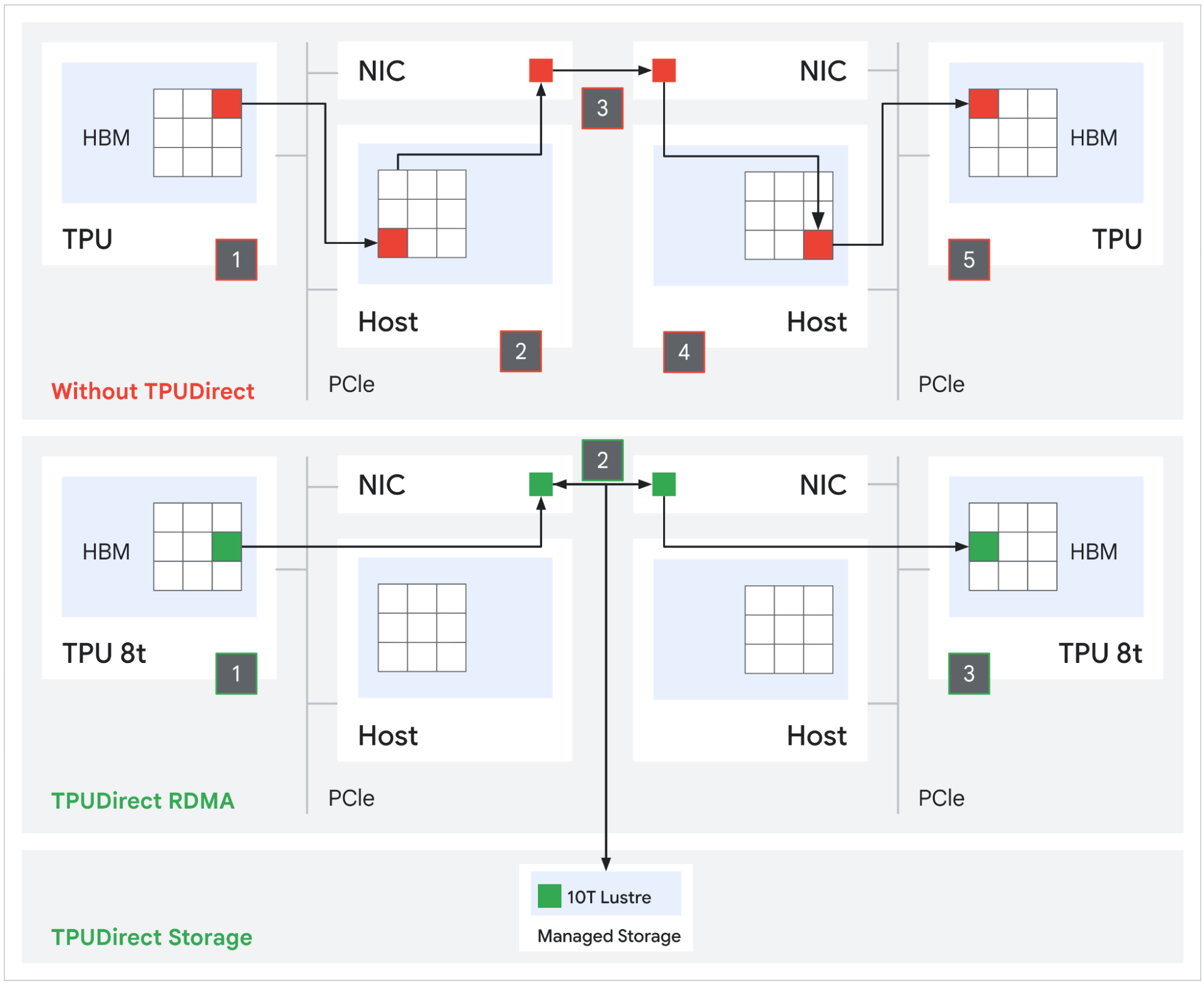
Prior TPU generations used a host-mediated path for network and storage I/O: packets landed in host DRAM first, then a separate DMA copied them into TPU HBM. That is two memory transactions with the host CPU in the loop. TPUDirect RDMA eliminates the bounce buffer. The NIC reads and writes TPU HBM directly via PCIe peer-to-peer, removing the host from the data path. NVIDIA has offered the equivalent capability with GPUDirect RDMA for years and quotes roughly 10x improvement over the host-mediated path. Google is now matching that on the TPU side.
Source: Google
TPUDirect Storage extends the same principle to persistent storage. Tensors move directly between TPU HBM and Managed Lustre at an aggregate rate of 10 TB/s, which Google claims delivers 10x faster storage access than the equivalent path on Ironwood. At the frontier scale, where checkpoints can run into the hundreds of terabytes, the difference is whether a multi-week training run streams checkpoints and datasets at line rate or stalls the MXU pipeline waiting on host I/O.
Arm Axion Hosts
Every prior TPU generation ran on third-party x86 hosts. 8t is the first to use Google’s own Axion processor, an Arm Neoverse V2-based CPU, as the system header. The host CPU’s job on a TPU pod is real and gets harder at frontier scale: it drives the input pipeline, decodes and shuffles multi-petabyte datasets, manages the JAX/XLA control plane, handles checkpoint serialization, and coordinates SPMD dispatch across thousands of chips. If the host stalls, the MXU sits idle.
Google specifically calls out Axion-powered NUMA isolation on 8t as the mechanism keeping host-side jitter from leaking into the synchronized collective phases of training. At 9,600 chips per pod, even small per-host hiccups compound into measurable loss of goodput. TPUDirect handles the data-path side by removing the host from bulk transfers. Axion handles the control-path side by giving each TPU enough dedicated CPU bandwidth so that preprocessing never becomes the bottleneck. Google has also increased the ratio of physical Axion hosts per server on the eighth-generation platform, giving the orchestration overhead, which scales with chip count, more headroom than Ironwood’s host configuration provided.
TPU 8i “Zebrafish”
The inference chip shares 8t’s Axion host platform, native FP4, and HBM3e memory generation, but the silicon underneath targets a different bottleneck. Training is compute-bound; inference decode is memory-bandwidth-bound. Most of 8i’s architectural differences follow from that.
The largest change is on-chip SRAM. 8i carries 384 MB of Vmem, three times as much as Ironwood had. The reason this matters is KV cache. During long-context decoding, each generated token requires reading the accumulated key-value states from prior tokens. On most accelerators, that read comes from HBM, which means decode throughput is gated by memory bandwidth rather than compute. 8i is sized to hold meaningful KV cache footprints entirely on silicon. On-chip SRAM bandwidth is roughly an order of magnitude higher than HBM, so every KV read served from SRAM rather than HBM means shorter per-token latency and higher tokens-per-second at the same power.
Source: Google
The TensorCore configuration is the other major departure. Where 8t uses a single TensorCore at 12.6 PFLOPS, 8i splits compute across two TensorCores at a combined 10.1 PFLOPS. Lower peak throughput sounds like a downgrade until you consider what inference actually looks like at the chip level. Training workloads are batch-dominated: large matmuls amortize fixed overhead, and a single large MXU can sustain near-peak utilization. Inference decoding is the opposite. Batch sizes are small, per-token compute windows are short, and the chip spends a material fraction of its time on collectives, sampling, and routing rather than pure matmul. A single large engine stalls during those irregular gaps. Splitting into two TensorCores lets 8i overlap compute phases more effectively, with each TensorCore fed by its own four directly attached HBM stacks, totaling 288 GB at 8.6 TB/s across the package. The result is higher sustained utilization at the batch sizes that actually run in interactive serving.
At the scale-up domain level, the 1,024 active chips in a Boardfly pod aggregate to roughly 295 TB of HBM, 384 GB of on-chip SRAM, and 10.3 EFLOPS of FP4 compute. The SRAM number is the one that matters most for inference: 384 GB of on-chip cache across the domain is enough to hold substantial KV state without touching HBM, which is what makes long-context serving at low latency viable.
The host side follows the same logic. Google says it has increased the number of physical Axion hosts per server on 8i compared to Ironwood. Inference servers spend a nontrivial fraction of per-token time on tokenization, sampling logic, routing, batching, and agent runtime orchestration. These overheads scale with concurrency rather than model size, and at the request rates that agentic workloads generate, the host can become the bottleneck. More host CPU per accelerator is the straightforward fix.
Collectives Acceleration Engine
The other major on-die change is the Collectives Acceleration Engine, which replaces the four SparseCores that Ironwood carried. SparseCores handle MoE routing and embedding lookups with dedicated gather-scatter hardware, so removing them from the inference chip signals that 8i optimizes for a different bottleneck.
The bottleneck CAE addresses is collective latency. Every decoded token requires the participating chips to synchronize: attention outputs must be all-reduced, expert routing metadata must be broadcast, and sampled tokens must propagate to the next step. On GPUs, this coordination happens in software through NCCL, which schedules collectives as a sequence of kernel launches and network operations. On 8i, the CAE is a dedicated silicon sitting on its own chiplet die alongside the TensorCores, handling these synchronization primitives in hardware.
Google claims up to 5x lower on-chip collective latency versus Ironwood. At training-scale batch sizes, that improvement would be swallowed by compute time; the collective is a small fraction of the step. At the small batches and short per-token windows of interactive inference, collective latency can dominate per-token time, so the 5x reduction shows up in tokens per second and price per token.
8i also moves from the 3D torus topology to what Google calls Boardfly, a Dragonfly-inspired hierarchical topology that trades ring-collective bandwidth for all-to-all latency. We will examine Boardfly in detail below.
Boardfly Topology
8i uses a different topology than 8t because training and inference have different communication patterns.
The 3D torus is ideal for ring collectives: each chip has six neighbors, data rotates around the ring, and no chip routes arbitrary traffic. Training is dominated by these ring-friendly patterns, which is why 8t retains the torus. A ring all-reduce maps perfectly to a single torus axis. Frontier jobs typically place data parallelism on one axis, tensor parallelism on another, and pipeline parallelism on the third. The topology and the workload are matched.
Inference serving a large MoE model has a different communication profile. Experts are pinned across many chips, and every decoded token triggers an all-to-all: tokens must reach their assigned experts scattered across the fabric, and expert outputs must return. This is not a ring. It is arbitrary point-to-point traffic, and on a 1,024-chip 3D torus, the worst-case path between any two chips is 16 hops. Google breaks down this math for us “In a 3D torus, nodes are arranged in a grid where each dimension wraps around like a ring. To reach the furthest possible chip in a 8 x 8 x 16 (1024-chip) configuration, a packet must traverse half the distance of each ring:
3D torus = 8/2(X) + 8/2(Y) + 16/2(Z) = 16 hops
While the torus is highly efficient for the neighbor-to-neighbor communication typical of dense training, it creates a latency tax for all-to-all communication patterns. In the era of reasoning models and MoE, where any chip may need to talk to any other chip to route a token, this hop count matters.”
For latency-sensitive interactive serving, those extra hops push per-token latency outside its SLO.
Source: Google
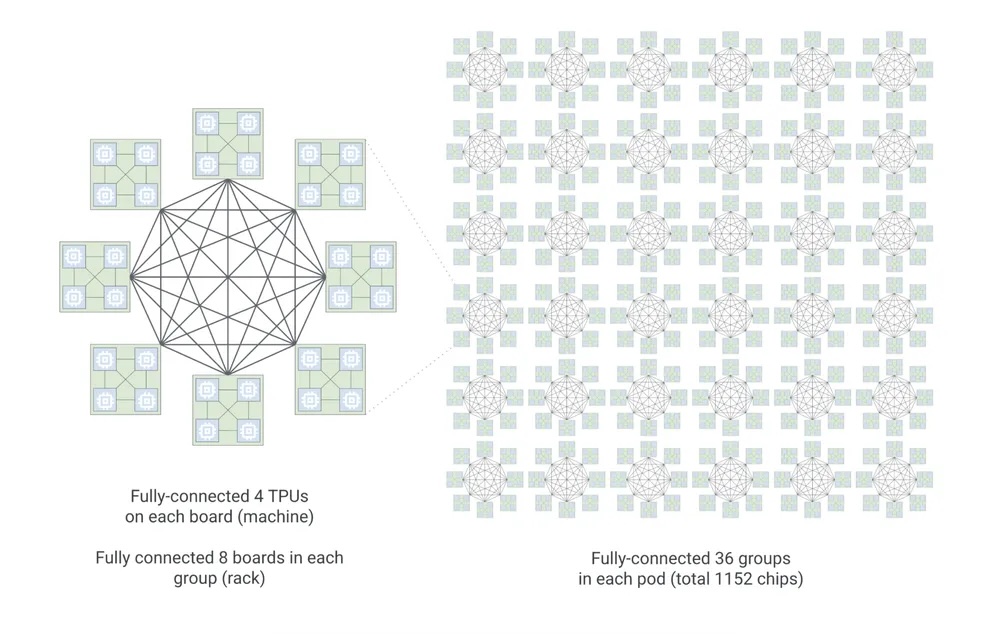
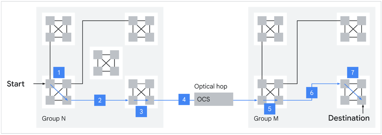
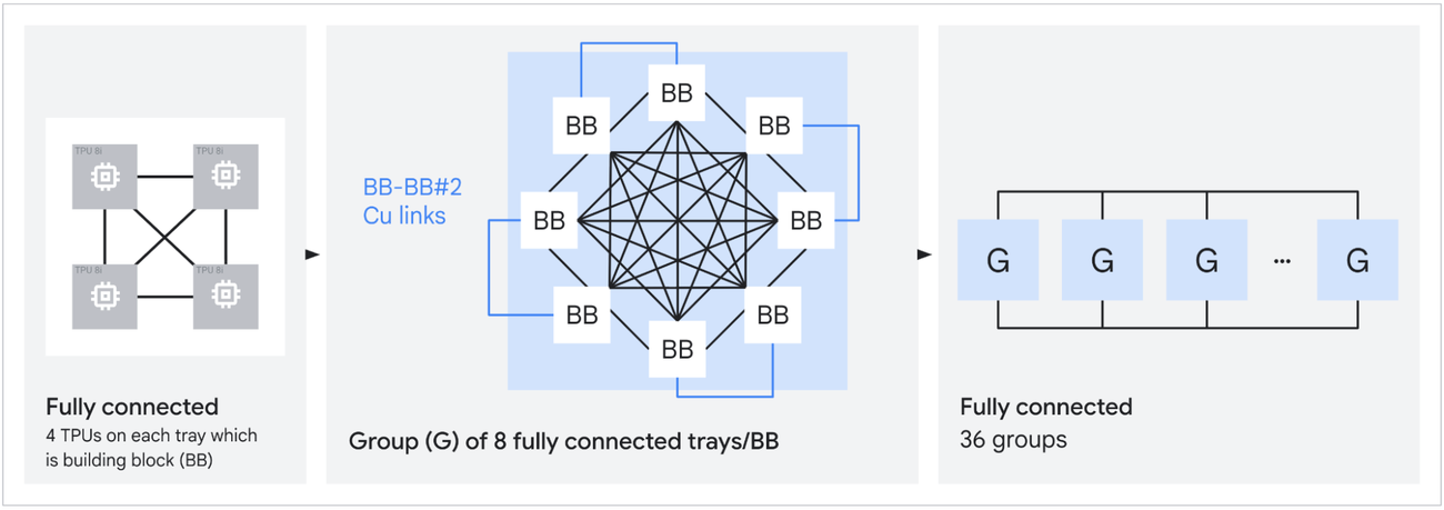
Boardfly is a Dragonfly-inspired hierarchy designed to compress that diameter. The structure has three levels. The building block is a four-chip ring with 16 external connections. Eight of these building blocks form a group, fully connected via copper cabling with 11 links per group. Thirty-six groups connect through Optical Circuit Switches to form a pod. The result is a 1,152-chip scale-up domain (1,024 active) with a maximum of 7 hops between any two chips, a 56% reduction from the torus. Google claims this yields up to 50% improvement in latency for communication-intensive workloads like MoE all-to-all.
The larger scale-up domain also matters for expert replication. More chips per ICI fabric means each expert in a large MoE can be replicated more times, which smooths routing imbalance and keeps decode latency flat when token distribution is skewed. Top-k routing is data-dependent; some experts will see more tokens than others on any given step. Replication absorbs that variance. ICI bandwidth was doubled to 19.2 Tb/s per chip in part to handle the resulting traffic.
Virgo Network
A 9,600-chip superpod is large, but frontier training runs increasingly require more. Virgo is the scale-out fabric that connects superpods within a data center, handling east-west RDMA traffic between pods when a job outgrows a single scale-up domain.
A single Virgo fabric links more than 134,000 8t chips at 47 Pb/s of non-blocking bisectional bandwidth, up to 4x the per-accelerator bandwidth and 40% lower unloaded latency compared to the previous generation. The architecture is a flat, two-layer non-blocking topology built on high-radix switches with a multi-planar design and independent control domains.
Traditional Clos fabrics oversubscribe at higher tiers to keep port counts and costs manageable. That works fine when most traffic is north-south, which is the pattern in general-purpose cloud: clients hit load balancers, load balancers hit application servers, application servers hit storage. AI training workloads are almost entirely east-west, chip-to-chip across the fabric, and the collectives are bisection-dominated. Any oversubscription at any tier drops straight into training step time. Virgo’s flat two-layer design with high-radix switches eliminates the spine-tier bottleneck by building switches with enough ports per ASIC to terminate a meaningful fraction of the fabric in two hops.
The reliability engineering matters at this scale and depends heavily on Google’s MEMS-based Optical Circuit Switches. OCS lets Google reconfigure the physical topology between jobs without rewiring anything, and more critically, route around failed chips or links mid-run. When a failure is detected, OCS can remap the affected portion of the fabric in milliseconds, eliminating the need for manual intervention. Sub-millisecond telemetry feeds automated straggler and hang detection. The combination of fast detection and OCS-based rerouting optimizes mean time between interrupts and mean time to recovery at 100,000+ chip scale, where the statistical certainty of some failure during a multi-week run approaches 100%. The 97% goodput target Google quotes for 8t pods depends on this infrastructure. The same OCS technology appears throughout the TPU stack: it stitches cubes into superpods at the ICI layer, connects Boardfly groups at the 8i scale-up layer, and handles inter-pod traffic at the Virgo layer.
At 134,000 chips, the aggregate compute reaches roughly 1,690 EFLOPS of FP4, or about 1.7 ZFLOPS. Google states that the architecture supports near-linear scaling for up to a million chips in a single logical training cluster, though current deployments have not yet reached that ceiling.
Jupiter and Multi-Data-Center Scale
Virgo handles east-west accelerator traffic within a data center, but it is not the top of the stack. Jupiter is Google’s existing north-south fabric, now in its fifth generation, which handles front-end traffic and access to distributed storage and compute resources. Jupiter was not announced at Cloud Next; it is the existing infrastructure that the 8 generation builds on.
The latest Jupiter iteration delivers 13 Pb/s of bisectional bandwidth per data center building with 99.999% availability, using Apollo MEMS OCS switches at roughly 108 W per OCS versus roughly 3,000 W for an equivalent electrical packet switch. This is the fabric that connects Google’s data centers to the outside world and to each other.
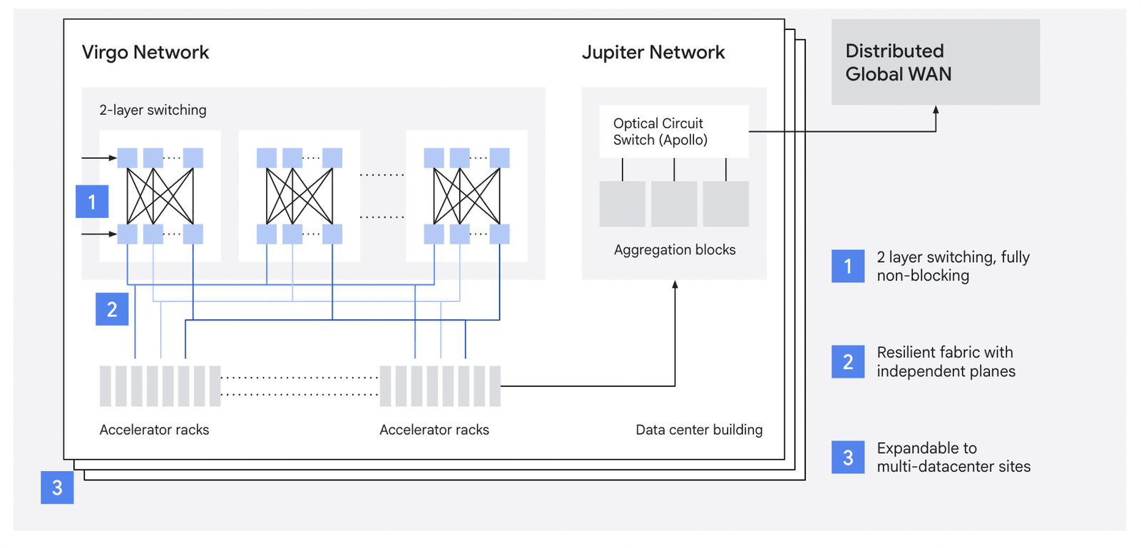
For training runs that exceed the power and space of a single data center, Jupiter is what enables scaling across multiple sites. The combination is layered: ICI within a pod, Virgo between pods within a site, Jupiter between sites. Google’s Pathways software stack can address workloads across these multi-data-center domains as a single logical cluster.
At ~1.7 ZFLOPS, a single Virgo fabric is the largest announced AI training cluster. Multiple Virgo fabrics linked by Jupiter can address over a million TPU chips, which is the scale Google is targeting, even if current deployments have not reached it.
Goodput and Utilization
Raw FLOPs matter less than the fraction of those FLOPs that produce useful work. Google quotes a 97% goodput target for 8t superpods, meaning 97% of wall-clock time is spent on productive compute rather than recovery, stalls, or coordination overhead. That number depends on the OCS-based fault tolerance and sub-millisecond telemetry covered above.
Model FLOPs Utilization (MFU) is the other variable. MFU measures what fraction of peak theoretical FLOPs the chip actually sustains on a real workload. SemiAnalysis estimates that at 40% TPU MFU, the cost per effective training FLOP drops by roughly 62% compared to GB300 NVL72, with breakeven at roughly 15% TPU MFU. Anthropic’s publicly disclosed TPU economics suggest they operate well above that breakeven. The combination of high goodput (keeping chips running) and competitive MFU (keeping chips busy when running) is what makes TPU TCO work at scale.
Where 8 Sits
Comparing TPU 8 to NVIDIA’s current and upcoming platforms requires careful attention to units. NVIDIA quotes NVLink bandwidth as bidirectional aggregate; a B200 at 1.8 TB/s NVLink 5 is 900 GB/s per direction. NVIDIA’s headline FLOPs are usually 2:4 sparse; dense is half that. Google’s TPU numbers are dense and bidirectional. When reading any comparison, check whether the bandwidth is unidirectional or bidirectional and whether the FLOPs are dense or sparse.
Per-chip FP4, 8t at 12.6 PFLOPS dense sits between GB200’s 10 PFLOPS sparse (5 PFLOPS dense) and GB300’s 20 PFLOPS sparse (15 PFLOPS dense). The per-chip comparison is close. The scale-up comparison is not. A GB300 NVL72 rack carries 72 GPUs in one NVLink domain. A 8t superpod consists of 9,600 chips in a single 3D torus. That is 133x more chips in a single collective domain, which is the gap that separates the platforms for frontier training.
NVIDIA is not standing still. Vera Rubin ships in H2 2026 with 50 PFLOPS of NVFP4 inference per package (though SemiAnalysis has questioned whether that number assumes adaptive compression), 288 GB of HBM4 at 22 TB/s, and NVLink 6 at 3.6 TB/s bidirectional. Rubin Ultra in H2 2027 stitches four reticle dies for up to 100 PFLOPS FP4 and 1 TB of HBM4e per package. Kyber NVL576 will bind 576 Rubin Ultra GPUs in a single rack at 15 EFLOPS FP4 inference. That starts to narrow Google’s scale-up advantage, though 576 GPUs is still an order of magnitude smaller than a 8t superpod.
Where 8 leads: scale-up domain size (9,600 chips versus 72 GPUs, or 576 post-Kyber), single-fabric scale (134,000+ chips at 47 Pb/s), deterministic latency from static XLA scheduling, and TCO for workloads that fit the TPU model.
Where 8 trails: per-chip HBM capacity (216 GB versus Rubin’s 288 GB HBM4), sparsity (NVIDIA has a 2:4 hardware path, Google does not), and ecosystem breadth (CUDA, cuDNN, TensorRT-LLM, and the PyTorch-first serving stack land on NVIDIA first; native PyTorch on TPU is still preview).
Both platforms have demand. Meta is reportedly in discussions for a multi-billion-dollar deal to deploy Google TPUs in its data centers starting in 2027, with potential Cloud TPU rentals as early as 2026. At the same time, Google Cloud announced A5X instances built on NVIDIA Vera Rubin NVL72, scaling to 80,000 Rubin GPUs within a single site and 960,000 GPUs across multi-site deployments. Google is building out both at scale.
Wrap Up
The eighth-generation TPU is two chips rather than one, built for what large-scale training and agentic inference look like now rather than for general-purpose AI workloads. 8t pushes scale-up to 9,600 chips per superpod and scale-out to 134,000+ chips per Virgo fabric. 8i trades SparseCores for collective-acceleration silicon and swaps the 3D torus for Boardfly to meet the latency targets required by MoE serving at scale. NVIDIA’s roadmap, with Vera Rubin, Rubin Ultra, and Kyber, will narrow some of these gaps over 2026-2027, but the scale-up domain advantage persists for now. For frontier labs running mixture-of-experts models on hundreds of thousands of chips, 8 is a credible alternative to Grace Blackwell, and Meta’s discussions suggest the market is starting to price that in.


 Amazon