

The LPU, or Language Processing Unit, is a custom AI inference accelerator designed and built by Groq, Inc. Founded in 2016 by Jonathan Ross, a former Google engineer credited as one of the original inventors of the TPU, Groq spent years developing a deterministic, software-defined processor architecture from the ground up. Unlike GPUs, which rely on dynamic hardware scheduling and multi-level cache hierarchies, the LPU takes a radically different approach: it eliminates all reactive hardware components and places the entire control plane in the compiler, enabling fully predictable execution down to the clock cycle.
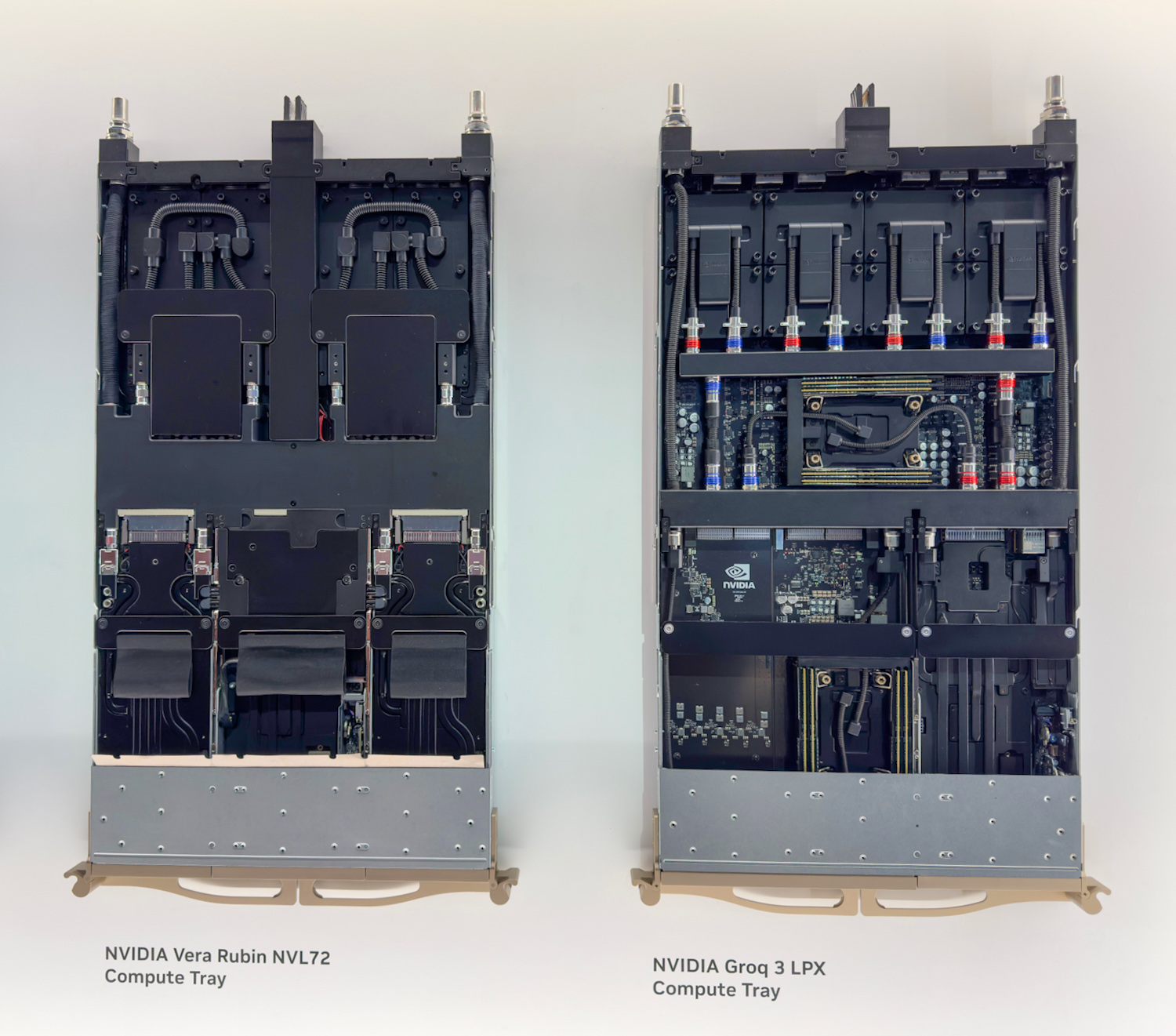
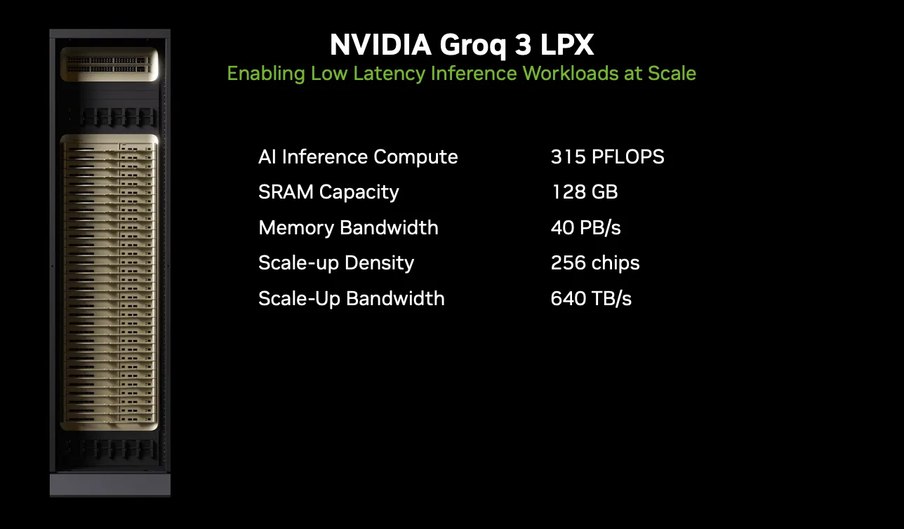
In December last year, NVIDIA acquired Groq, bringing the LPU architecture under the NVIDIA umbrella. The acquisition was enormously popular in the industry and sparked immediate speculation about how NVIDIA would integrate Groq’s technology into its data center ecosystem. Those questions were finally answered at GTC 2026, where NVIDIA unveiled the Groq 3 LPX as the seventh chip of the Vera Rubin Platform, pairing 256 LPU accelerators in a rack-scale system alongside the Vera Rubin NVL72.
What Happened to CPX?
Last year at the AI Infra Summit, NVIDIA also announced the CPX rack in a couple of configurations designed for accelerating long-context inference queries. After our initial coverage of that announcement, it raised several questions for us about the CPX’s actual function. At first glance, although it was an interesting architectural concept, the CPX didn’t appear to offer anything materially beyond the Rubin GPU itself, aside from perhaps additional acceleration for attention operations. Then came the Groq acquisition, which sparked speculation about how NVIDIA would integrate Groq’s LPU technology into the broader Vera Rubin platform.
Well, NVIDIA cleared the air at GTC 2026 with the LPX announcement. From what was presented, it appears that the CPX rack concept has evolved into the Groq 3 LPX Rack, with the original CPX’s context-processing focus giving way to a fundamentally different decode-acceleration architecture built around Groq’s silicon. The LPX Rack is fully liquid-cooled, built on MGX infrastructure, and will be available in the second half of 2026, coincident with the broader Vera Rubin rollout. NVIDIA claims up to 35x higher inference throughput per megawatt and up to 10x more revenue opportunity for trillion-parameter models with this new addition.
But more importantly, NVIDIA confirmed that the LPU operates as an accelerator within the existing CUDA stack running on the Vera and NVL72 platforms, with computation offloaded transparently on a per-token basis. During the GTC Q&A, NVIDIA described the LPU as a “decode model booster” and explained that they will be working closely with AI labs and frontier model builders deploying trillion-parameter models to enable the next generation of premium model serving.
With the CPX question settled, the natural follow-up is: what exactly is this LPU that NVIDIA is building an entire rack-scale system around?
What Is an LPU?
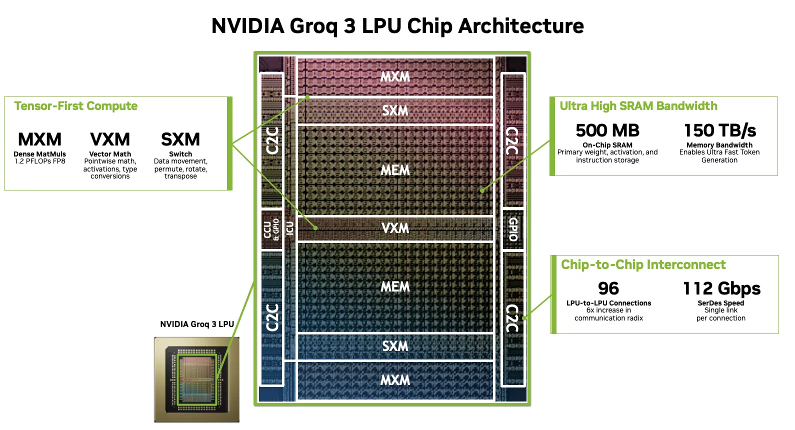
At its core, the LPU is a very large vector processor. The fundamental unit of both computation and communication is a 320-element vector consisting of 320 bytes at INT8, 640 bytes at FP16. Every operation on the chip, whether arithmetic, memory access, data reshaping, or inter-chip transfer, operates on these fixed-size vectors.
Source: Nvidia
The architecture is built from a single foundational building block: a SIMD functional unit paired with a lightweight instruction dispatch unit. Groq treats this as a base class that gets specialized into four distinct types, each optimized for a specific category of operations:
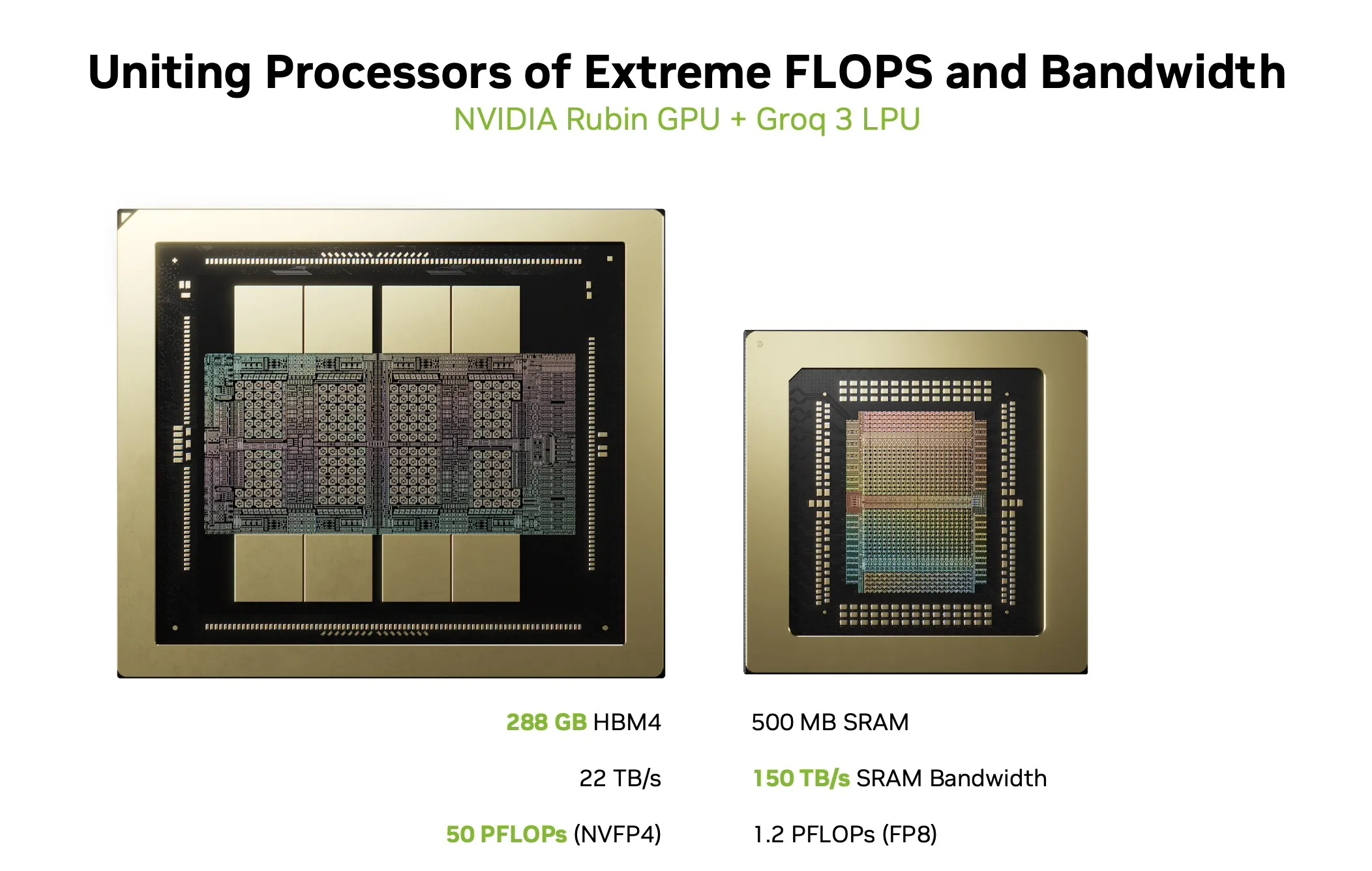
Matrix Execution Modules (MXM): The primary compute workhorse, providing dense multiply-accumulate capability for matrix-vector and matrix-matrix operations. Each of the 8 Groq 3 LP30 chips in NVIDIA’s LPX rack delivers 1.2 PFLOPS of FP8 compute per chip, totalling 9.6 PLOPS of FP8 compute per LPX tray.
Vector Execution Modules (VXM): Handle pointwise arithmetic, logical operations, type conversions, and activation functions. The VXM contains an array of ALUs that the compiler automatically chains to form compound operations (for example, reduction followed by bias-add, followed by activation, followed by type cast) in a single pass.
Switch Execution Modules (SXM): Perform structured data movement, including permutation, rotation, distribution, and transposition of vectors.
Memory Units (MEM): A flat, SRAM-first memory architecture with no caches, no hierarchy, and no concept of a cache miss. The Groq 3 LP30 provides 500 MB of on-chip SRAM at 150 TB/s bandwidth. The compiler directly addresses physical bank locations, knowing the exact position of all data throughout program execution.
Multiple copies of each functional unit type are stamped across the horizontal dimension of the chip. Instructions flow from top and bottom to the middle while data streams flow east to west, intersecting the functional units to perform operations.
The 1D Interconnect, Stream Registers, and Determinism
Stream Registers and the 1D Interconnect
Communication between functional units on the LPU occurs via stream registers, a deliberately simple one-dimensional interconnect. Two communication paths exist, one flowing eastward and one westward, with each stream register representing a single hop. Data moves at exactly one hop per clock cycle, which means the compiler can reason about travel time between any two functional units by performing a simple add or subtract based on their physical positions on the chip layout.
There are no queues and no contention mechanisms within the interconnect. This simplifies the scheduling problem from a complex 2D bin-packing problem into a far more tractable 1D problem. Igor Arsovski, Groq’s Chief Architect, describes it best: the compiler knows exactly where a piece of data will be 10 cycles from now, because it will be exactly 10 hops away. There is no ambiguity, no speculation, and no hardware making independent routing decisions.
Determinism
The defining characteristic of the LPU is determinism. Unlike conventional processors, where dynamic scheduling, cache behavior, and memory access contention introduce runtime variance, LPUs execute with zero variance, and every functional unit operates in lockstep.
This determinism is achieved by removing features like hardware interlocks and moving all decision-making into the compiler; the hardware simply executes the resulting schedule. Other benefits of this approach is everything operates with the exact same latency, and even power consumption is predictable at every point in time.
Determinism also extends to the numerical domain through what Groq calls TruePoint technology, where the architecture’s guaranteed order of operations enables FP32-level accuracy from FP16 inputs via a 320-element fused dot product with a single rounding step. The details of why numerical determinism matters for LLM inference, and why non-deterministic hardware produces subtly different outputs across runs, are explored in depth in Thinking Lab’s whitepaper “Defeating Nondeterminism in LLM Inference“. That is not the focus of this article, but readers interested in the implications for numerical accuracy can find the relevant analysis in Groq’s TruePoint technical documentation, linked at the end.
How LPUs Connect: RealScale, the Assembly Line, and Rack Topology
The Assembly Line: How Data Moves
At the simplest level, data movement across LPUs works like an assembly line. When a model is compiled for the system, the compiler partitions it into stages and spatially maps each stage onto a group of LPU chips. Each group stores the weight parameters it needs in local on-chip SRAM. During inference, the only data that travels between groups of chips is the intermediate activation output from the previous stage. Data flows from chip to chip like a product moving along a conveyor belt, with each station performing its assigned computation and passing the result to the next. This is fundamentally different from GPUs, where each compute stage requires retrieving the full weight set from off-chip HBM memory and writing results back. On the LPU, the weights are already resident in SRAM at each station; only the activation tensors move.
A Note on C2C Links: RealScale, Not NVIDIA C2C
Before getting into the topology details, it is important to clarify a potential source of confusion. The chip-to-chip (C2C) links used throughout the LPX system are Groq’s RealScale C2C interconnect. These are not the same as NVIDIA’s C2C technology, which is used elsewhere in the NVIDIA ecosystem. The two technologies are architecturally distinct:
- NVIDIA C2C is a cache-coherent interconnect designed for connecting two different chip types within a tightly coupled module, such as a CPU-to-GPU link. It uses a coherent protocol with higher-speed SerDes and is designed for heterogeneous chip-to-chip communication within a single package or module.
- Groq RealScale C2C is a software-scheduled, deterministic, point-to-point interconnect. Network links are explicitly flow-controlled by the compiler and scheduled as first-class functional units, just like the MXM or VXM compute units. There is no hardware arbitration or adaptive routing, and packets carry no source or destination headers. The links are phase-aligned and act like high-bandwidth, fixed-latency wires between chips. A plesiochronous protocol accounts deterministically for natural clock drift across chips, exposing a single common time domain to the compiler across the entire network.
Every C2C connection in the LPX rack, whether within a tray, across trays via the spine, or between racks via the front-panel ports, uses RealScale. This is the same fundamental interconnect technology Groq has used since the original GroqNode, scaled up in link speed (from 30 Gbps to 112 Gbps per lane) but architecturally unchanged.
Note: The next section explaining the connectivity is based on our understanding of the architecture based on Groq’s documentation (linked at the end), NVIDIA’s blog post, and the explanation of the rack provided to us at the GTC booth:
- The C2C links used by the LPX rack units are Groq’s technology and are not the same as the C2C links used in other rack-scale systems from NVIDIA
- The 4 C2C links at the front of each of the LPX rack units are used to connect to adjacent rack units at the same level
- Within a rack, there is all-to-all communication between LPUs
- The processor in the LPX rack is x86
Intra-Tray Connectivity
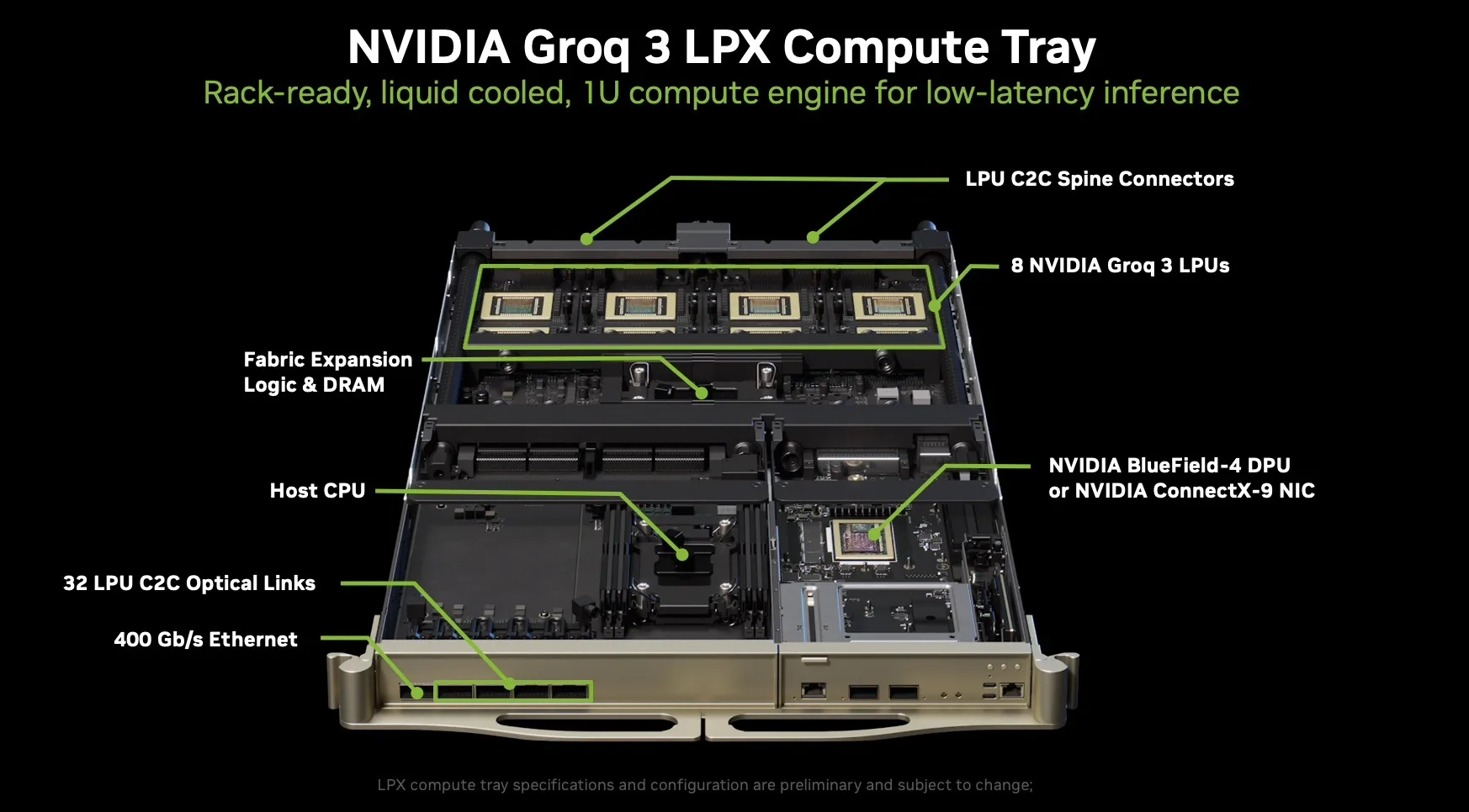
The fundamental building block of Groq’s network topology has not changed from the original GroqNode to the NVIDIA Groq 3 LPX. Each 1U compute tray contains exactly eight LP30 chips, densely interconnected in a complete graph (all-to-all), where every chip can directly communicate with every other chip at the same rate.
Source: Nvidia
Each LP30 chip has 96 C2C links, each running at 112 Gbps, providing 2.5 TB/s of bidirectional bandwidth per chip. In a complete graph of 8 chips, each chip has 7 neighbors. The number of unique chip-to-chip edges within a tray is C(8,2) = 28. Some portion of each chip’s 96 links is dedicated to these intra-tray all-to-all connections, with the remaining links routed to the backplane (for the rack spine) and the front panel (for inter-rack). NVIDIA’s published spec lists 20 TB/s of total scale-up bandwidth per tray, which represents the combined intra-tray and spine bandwidth. We can verify this: each tray has 8 chips × 96 links = 768 links in total. Subtracting the 32 front-panel inter-rack lanes leaves 736 links for scale-up. At 112 Gbps per link, that is 736 × 112 Gbps = 82,432 Gbps, or approximately 10.3 TB/s per direction, which works out to roughly 20.6 TB/s bi-directional. This aligns well with NVIDIA’s stated 20 TB/s per tray.
This 8-chip all-to-all group forms the “local group” of a dragonfly network topology. The original GroqChip 1 had 11 C2C links per card, each at 30 Gbps per lane (four lanes per link), for a total of 330 GB/s per card. The Groq 3 LP30’s 96 links at 112 Gbps represent a massive generational leap in per-chip I/O bandwidth while preserving the same topological structure.
Intra-Rack Connectivity
Within a single LPX rack, 32 compute trays (256 chips total) interconnect via four ETL spines in the backplane. These spines carry RealScale C2C traffic between trays, creating the rack-scale scale-up domain. The aggregate scale-up bandwidth across the full rack is 640 TB/s (32 trays × 20 TB/s per tray). Divided across the four spines, each spine carries approximately 160 TB/s of bi-directional bandwidth.
Inter-Rack Connectivity
Each 1U compute tray exposes four QSFP C2C ports on the front panel, providing a total of 32 lanes (8 lanes per port) for inter-rack communication. These ports connect to adjacent racks in a symmetric pattern: two ports (16 lanes) connect to the left adjacent rack, and two ports (16 lanes) connect to the right adjacent rack. Each U position connects to its corresponding U position in the neighboring rack (the first U in rack A connects to the first U in rack B, the second to the second, and so on).
Source: Nvidia
At 112 Gbps per lane, each tray’s 32 inter-rack lanes provide 32 × 112 Gbps = 3,584 Gbps, or approximately 448 GB/s per direction per tray of inter-rack bandwidth. Across the full rack, the 32 trays provide 32 × 32 = 1,024 inter-rack lanes. That works out to 1,024 × 112 Gbps = 114,688 Gbps, or approximately 14.3 TB/s per direction to each adjacent rack (split evenly: ~7.2 TB/s per direction to the left neighbor and ~7.2 TB/s per direction to the right neighbor).
This inter-rack bandwidth is sparser than the intra-rack bandwidth by design. Within the rack, the 640 TB/s scale-up domain provides dense, all-to-all reachability through the spine. Between racks, the front-panel links provide the sparser global connections of the dragonfly topology. This is the same architectural pattern as the original GroqRack, where four external C2C links per chip connected local groups (nodes) to form multi-rack systems with low network diameter (three hops maximum in a 264-chip deployment).
Putting It Together: Same Architecture, 4x the Density
The original four-rack GroqRack deployment contained 264 GroqChip processors. A single LPX rack packs 256 LP30 chips into one MGX ETL rack, roughly 4x the chip density collapsed into a single rack form factor with liquid cooling and a cableless backplane. The 8-chip all-to-all local group, the dragonfly topology, and the software-scheduled routing paradigm all carry forward intact. The fundamental Groq networking technology has not changed; it has been scaled.
For models that exceed the SRAM capacity of a single rack (128 GB total across 256 chips), multiple LPX racks or rows of racks can be interconnected via the front-panel C2C ports to extend the assembly line further. More on what this means for real-world model sizes in the next section.
Why FFN Layers? Understanding What NVIDIA Is Offloading
Why Decode Is Getting Harder to Serve
Before diving into the specifics of what NVIDIA is offloading to LPX and why, it helps to understand the broader trends, like NVIDIA points out, that make this architectural decision necessary. AI inference is not a single, uniform workload. Within a single request, the prefill phase (ingesting the prompt and building the KV cache) and the decode phase (generating tokens one at a time) place very different demands on hardware, and those demands shift with batch size, context length, and model structure.
As models produce longer reasoning outputs and multi-step chains of thought, a larger share of each request shifts into the sequential decode phase. At the same time, techniques like prefix caching reduce the cost of prefill by reusing shared prompt state across requests, which only makes the relative cost of decode more prominent. Context windows are also growing to hundreds of thousands of tokens, putting increasing pressure on memory bandwidth during attention computation. And in agentic workflows, latency compounds across many model calls, tool interactions, and verification loops. The cumulative effect is that decode latency is increasingly the bottleneck that users feel, and hardware optimized purely for maximum aggregate throughput is not always the best fit for workloads that require fast, predictable token generation for each individual request.
In addition, as seen with Anthropic’s Fast Mode release, lower latency and higher token throughput do drive higher revenues, with Anthropic’s fast inference offering costing 6x as much as regular requests.
With this LPX announcement, we know that NVIDIA wants to offload the biggest decode bottleneck to the LPUs: the feed-forward network (FFN) layers. To understand why FFN is the target and to appreciate the sheer scale of what that means, we analyzed the FFN parameter counts for today’s most popular open-source models.
What Are FFN Layers and Why Do They Dominate?
Every Transformer layer has two main blocks: an attention block and a feed-forward (FFN) block. The attention block lets tokens look at and mix information from other tokens in the sequence. The FFN block operates on each token independently: it projects the token’s representation up into a higher-dimensional space, applies a nonlinearity, and projects it back down. You can think of it as the model’s knowledge store, where factual associations and learned transformations live.
The MoE or Mixture of Experts architecture has emerged as the dominant architecture among today’s leading open-source large language models: DeepSeek R1, Kimi K2, Qwen3-235B, GLM-5, MiniMax M2.5, and OpenAI’s GPT-OSS 120B.
Within these MoE models, it is specifically the FFN block that gets replicated into hundreds of smaller independent copies called experts, while attention remains shared. A lightweight learned routing function dynamically selects a small subset of experts to activate on a per-token basis. The result is a model that stores an enormous total parameter count but only activates a fraction per token, getting the quality benefits of scale without the proportional compute cost.
However, as you must have realized, this poses another challenge: the FFN layers account for most of the model’s weights. For MoE models specifically, this can be as much as 90% of the model’s weights.
Inside DeepSeek R1: A Worked Example
To illustrate, let’s zoom into DeepSeek R1. The model has 61 Transformer layers with a hidden dimension (H) of 7,168. The first 3 layers use a standard dense FFN, while the remaining 58 use MoE (plus 1 additional MTP layer with its own experts, for a total of 59 MoE layers). Modern LLMs use a variant called SwiGLU, which has three weight matrices instead of two. The forward pass computes w2(SiLU(w1(x)) ⊙ w3(x)), where w1 (the gate projection) and w3 (the up projection) both expand the hidden dimension from H to an intermediate size I, and w2 (the down projection) compresses it back. The ⊙ is element-wise multiplication between the gated and ungated paths. None of these matrices has bias terms, so each SwiGLU FFN block contains exactly 3 × H × I parameters.
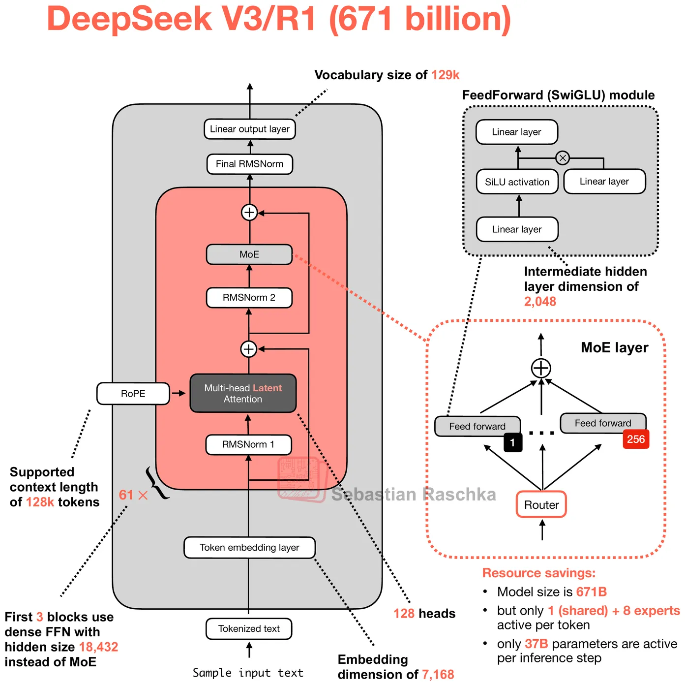
Source: Sebastian Raschka
For DeepSeek R1’s dense layers (the first 3), the intermediate dimension is 18,432, giving 3 × 7,168 × 18,432 = 396.4 million parameters per layer. For the MoE layers, each of the 256 routed experts is a complete SwiGLU block with a smaller intermediate dimension of 2,048, so each expert has 3 × 7,168 × 2,048 = 44.0 million parameters. Multiply by 256 experts, and you get 11.27 billion parameters in routed experts alone, per layer. On top of that, each MoE layer has one shared expert (same 44M-param SwiGLU block, always activated for every token), a router gate (a linear projection of shape [256, 7168] = 1.8M params), and a small bias vector of 256 FP32 values used for load balancing during routing.
The full FFN has approximately 669.1 billion parameters. In FP8 E4M3 format (1 byte per weight), that translates to roughly 623.1 GB of FFN data. That is 97.7% of the model’s estimated total size on disk. The remaining ~2.3% is attention weights, embeddings, the output head, layer norms, and FP8 scale metadata.
Decode Disaggregation
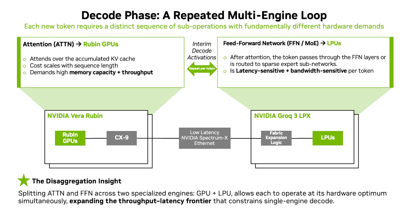
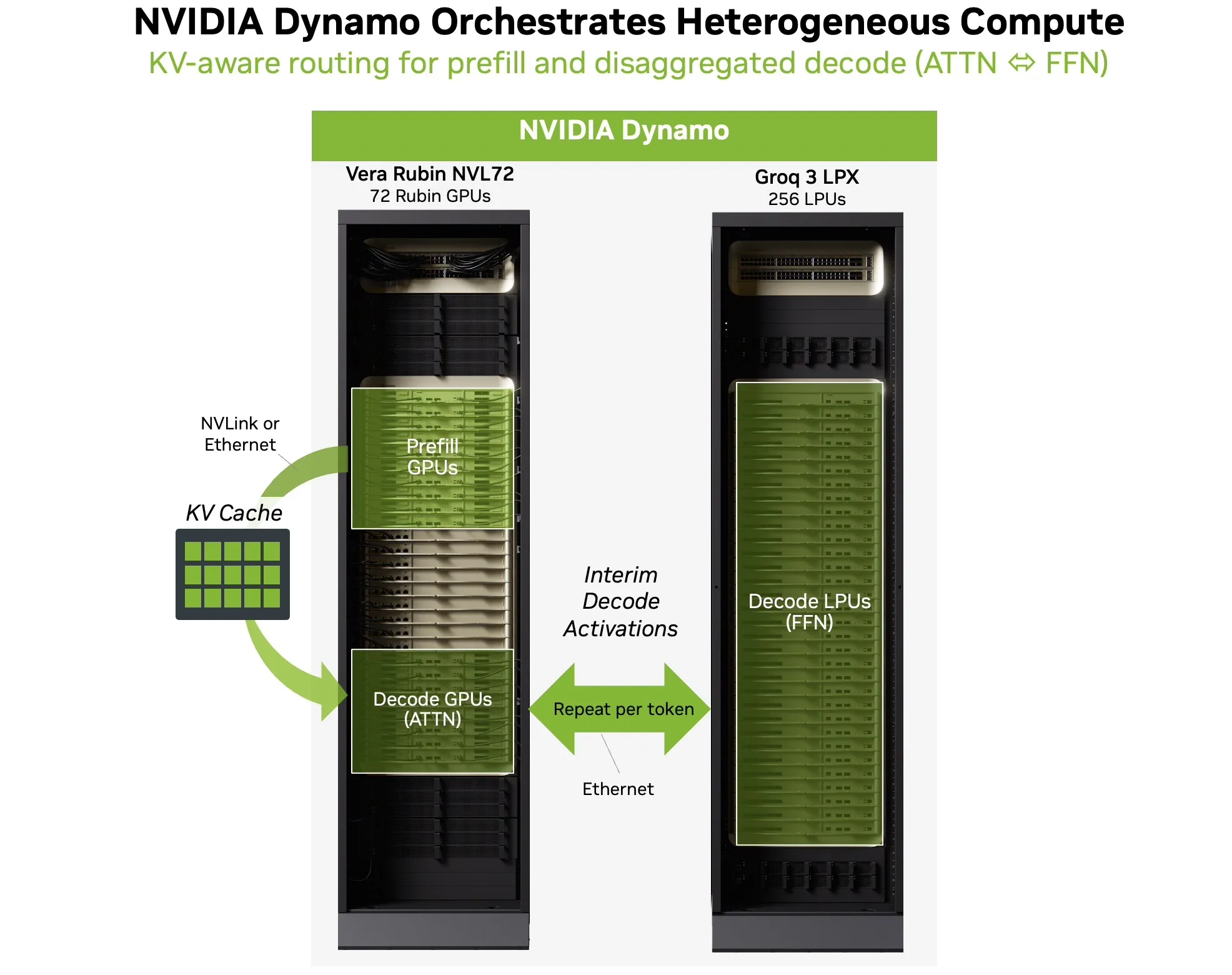
NVIDIA now frames the decode phase not as a monolithic operation but as a repeated per-token loop where different parts stress different hardware bottlenecks. The prefill phase is dominated by ingesting large inputs and building the KV cache, a workload that benefits from dense parallel compute and large memory capacity. The Vera Rubin NVL72 handles this efficiently, especially for long-context workloads where the prompt can be massive and highly variable.
Source: Nvidia
Decode is different. For each new token, the system must execute attention over the full accumulated KV cache and then run the FFN/MoE computation on the attention output. In NVIDIA’s Attention-FFN Disaggregation (AFD) architecture, these two steps are split across two engines. Rubin GPUs handle decode attention: reading the KV cache from HBM, computing the attention scores, and producing the intermediate activation. That activation tensor (what NVIDIA refers to as “interim tensor state”) is then handed off to the LPX, which runs the FFN or MoE expert computation at extreme bandwidth and deterministic latency before returning the result to the GPU to continue token generation.
This handoff happens for every single token. The activation tensors exchanged between GPU and LPU are small relative to the weight data, which is precisely the regime where the LPU’s near-zero-overhead networking excels. The split plays to each processor’s fundamental strengths: GPUs provide the HBM capacity and flexible execution needed for variable-length attention over large KV caches, while LPUs provide the SRAM bandwidth and deterministic scheduling needed for the bandwidth-bound, statically schedulable FFN weights.
Source: Nvidia
There is a subtle but important scaling property worth calling out here. As context length grows, the compute and memory requirements of the attention operation scale with it: the KV cache expands linearly with each additional token of context, and each new decode step must attend to the entire accumulated cache. FFN, however, does not grow with context at all. The FFN weight matrices (w1, w2, w3 in SwiGLU) are fixed constants of the model architecture. They are the same size whether the context is 1,000 tokens or 1,000,000 tokens, and each token passes through them independently. This means that in the AFD architecture, as context windows continue to grow, the GPU side absorbs the increasing cost (more HBM for KV cache, more compute for attention), while the LPX side remains completely static. The number of LPX racks required to serve a model’s FFN is determined entirely by the model’s architecture, not by the serving configuration’s context length. This neatly solves what was historically one of the biggest challenges for SRAM-only accelerators: that growing context demands eventually outstrip the fixed on-chip memory capacity. In the AFD split, the context-dependent work stays on hardware with expandable HBM, and the LPU handles only the context-independent work that fits naturally in fixed SRAM.
NVIDIA Dynamo makes heterogeneous decode operational
Making this two-engine loop work in production requires more than just hardware. NVIDIA’s Dynamo orchestration layer is what makes heterogeneous decode practical. Dynamo coordinates disaggregated serving across the GPU and LPU backends, handling the per-token classification, routing, and activation transfer required by AFD.
Source: Nvidia
In practice, Dynamo routes prefill to GPU workers to process the input and build the KV cache. During decode, Dynamo orchestrates the AFD loop: GPUs run attention over the accumulated KV cache, intermediate activations are handed off to LPUs for FFN/MoE execution, and outputs return to the GPUs to continue token generation. The result is a single coherent serving path rather than two disconnected systems.
Dynamo also provides KV-aware routing (so requests land on workers that already have the relevant KV cache resident), latency-target-driven scheduling (so interactive sessions are kept out of long queues), and low-overhead transfer management. These capabilities are important because, under real production traffic with variable context lengths, mixed request types, and bursty concurrency, the orchestration layer keeps tail latency stable and prevents cross-tenant jitter from degrading the user experience.
FFN Sizes Across All Major Open-Source Models and LPX Sizing
Now that we understand how LPX works, and what it’s trying to solve. Let’s look into what it means in terms of hardware requirements.
We calculated the number of parameters and FFN size on disk for popular models using config.json and model.safetensors.index.json available on Huggingface.
| Model | FFN Params | FFN Size (on disk) | FFN % | Dtype | Experts |
|---|---|---|---|---|---|
| DeepSeek R1 and DeepSeek V3.2 | 669.1B | 623.1 GB | 97.7% | FP8 | 256 |
| Kimi K2 | 1.02T | 948.0 GB | 98.9% | FP8 | 384 |
| Kimi K2.5 | 1.02T | 474.0 GB | 98.5% | INT4 | 384 |
| MiniMax M2.5 | 224.7B | 209.3 GB | 97.7% | FP8 | 256 |
| OpenAI GPT-OSS 120B | 114.7B | 53.4 GB | 95.4% | MXFP4 | 128 |
| GLM 5 | 738.1B | 1,374.8 GB | 98.0% | BF16 | 256 |
| Qwen3 235B-A22B | 227.2B | 423.1 GB | 96.6% | BF16 | 128 |
The pattern confirms what we explored earlier: across every model in this analysis, FFN parameters account for 95% to 99% of the total model size on disk. Kimi K2 is the most extreme case, with 384 routed experts per layer pushing FFN to over 1 trillion parameters and nearly 99% of the total. Even the smallest model in the set, OpenAI’s GPT-OSS 120B with 128 experts stored in MXFP4, still has FFN representing 95.4% of the total. The on-disk sizes range from a modest 53 GB for GPT-OSS 120B (thanks to 4-bit quantization) up to nearly 1.4 TB for GLM 5 (stored in BF16 with no quantization).
These numbers help us understand the LPX sizing. A single LPX rack provides 128 GB of total SRAM across its 256 chips. For a model like OpenAI’s GPT-OSS 120B at 53 GB FFN, the FFN weights fit comfortably within a single rack with room to spare. DeepSeek R1 at 623 GB would require roughly five LPX racks, while GLM 5 at 1.4 TB in BF16 would need over ten (though quantizing to FP8 would cut that roughly in half). This is precisely why the inter-rack front-panel C2C ports are required: they allow multiple LPX racks to be chained together, extending the assembly line to accommodate larger models.
Accelerating Speculative Decoding with LPX
Beyond the AFD decode loop, NVIDIA identifies a second major use case for the LPX: serving as the draft-generation engine in speculative decoding.
Speculative decoding is an increasingly important technique for reducing latency in LLM inference. The idea is straightforward: a smaller, faster draft model generates multiple candidate tokens in advance, while a larger target model verifies and accepts them in parallel. When the draft model’s predictions are correct (which they often are for routine text), multiple tokens can be committed at once in a single verification step. The result is significantly higher effective tokens per second and lower perceived latency for the end user.
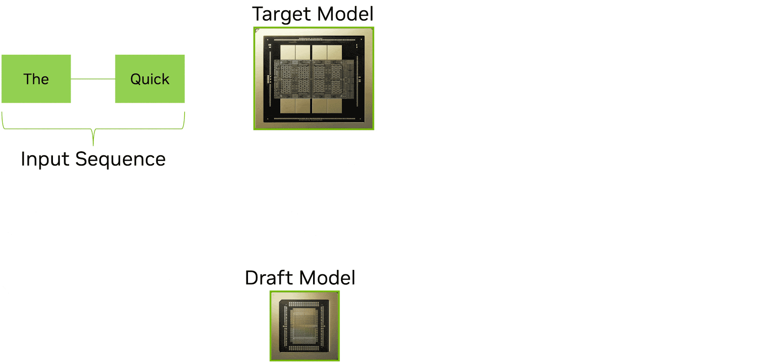
Source: Nvidia
The challenge is that speculative decoding requires the draft model to run extremely fast. Every millisecond the draft model spends generating candidates is a millisecond the verifier is waiting. On a conventional GPU-only setup, both the draft model and the target model compete for the same hardware resources, and the draft model’s speed is limited by the same HBM bandwidth constraints that affect everything else.
LPX is well-suited to this role. The deterministic execution model and the LP30’s extreme on-chip SRAM bandwidth enable very fast, predictable draft token generation. A smaller draft model fits comfortably in the SRAM of a single LPX tray or a small number of trays, and the deterministic scheduling ensures that draft generation runs at a consistent, predictable speed without the variance that would make it difficult to pipeline with the verifier.
In this configuration, the system pairs the two processors for complementary roles: LPX generates draft tokens rapidly using its low-latency architecture, while Rubin GPUs verify and finalize tokens efficiently using their high-throughput compute and large HBM capacity. This separation allows speculative decoding to run across heterogeneous processors rather than requiring both models to share a single GPU, potentially improving draft speed and verification throughput compared to a homogeneous setup.
NVIDIA has highlighted speculative decoding, alongside AFD, as a key workload for the LPX, suggesting it sees this as a significant part of the system’s value proposition. As frontier models continue to grow and reasoning chains lengthen, the ability to generate and verify tokens in parallel on specialized hardware could become an important lever for maintaining interactive responsiveness.
Final Thoughts: Extreme HW/SW Co-Design
One of the things that stands out about NVIDIA’s approach with the Vera Rubin platform and LPX is how precisely targeted each component is. In the consumer space, we regularly encounter products that try to solve problems no one actually has, from companies that do not deeply understand their customers’ needs. NVIDIA’s strategy here is a stark contrast. It is brutally obvious that they understand the inference pipeline’s problems at an extremely granular level, and they are optimizing every segment of that pipeline to help their customers maximize their return on the hardware.
The attention/FFN disaggregation is not a marketing concept. It is a direct response to the measured bottleneck profile of trillion-parameter MoE model serving. The decision to offload FFN specifically (and not attention) and evolving the CPX rack into the LPX rack reflects a precise understanding of which operations are bandwidth-bound versus capacity-bound, which are statically schedulable versus dynamically variable, and which processor architecture is best suited to each. The Dynamo orchestration layer, the transparent CUDA integration, and the cableless MGX rack design all point to an engineering organization that has thought through the full deployment lifecycle.
There are still many unknowns with LPX and NVIDIA’s new frontier products. One of the big lingering questions for us is what is the purpose of the “Fabric Expansion Logic and DRAM” what sort of Silicon is being used for it, and as many have already spotted the x86 socket, from the investment in Intel last year and the heatsink retention design it is likely an Intel processor but what part is still a big unknown.
The LPX deployment will initially focus on model builders and service providers rather than broad availability. And real-world performance under production traffic patterns, with variable context lengths, mixed request types, and bursty concurrency, and the power efficiency remains to be validated independently. We look forward to gaining access to these systems for independent testing.
Sources Referenced:
Groq: What is a language processing unit?
Groq: The Groq LPU, AI Inference Technology, Delivers More Energy Efficiency…
Groq: RealScale Chip-to-Chip Interconnect Technology
Groq: Low Latency for Real-time AI and HPC
Groq: Determinism and the Tensor Streaming Processor
Nvidia: Inside Nvidia Groq 3 LPX…
Aleksa Gordić – The AI Epiphany: How does Groq LPU work? (w/ Head of Silicon Igor Arsovski!)


 Amazon