

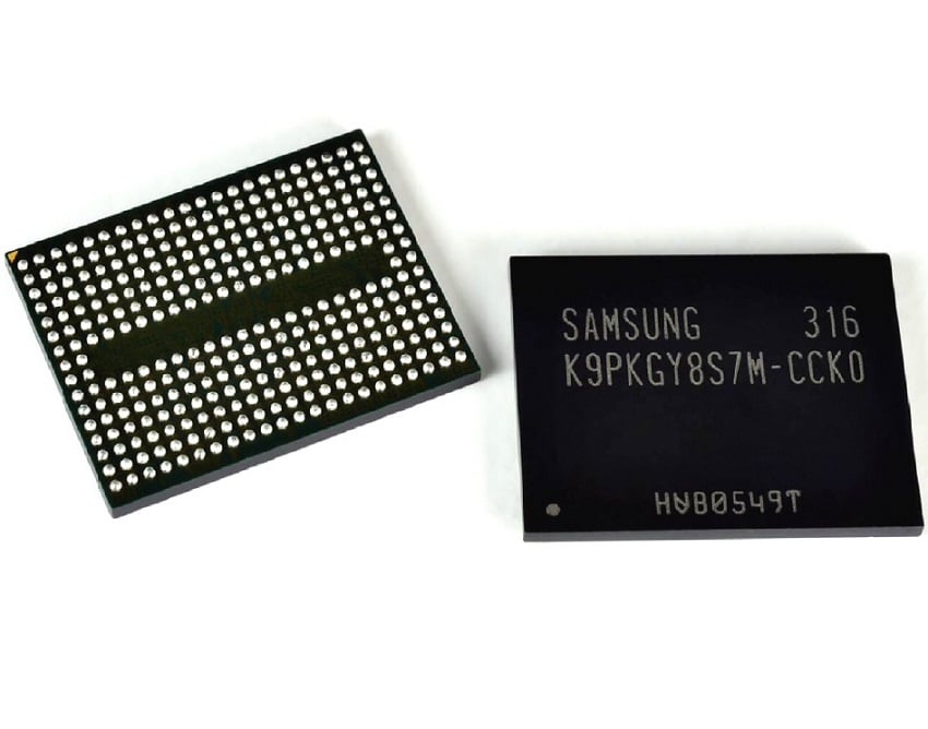
Samsung is announcing that is has begun mass production of its new 3D V-NAND which promises to bring anywhere from two to ten times the reliability and two times the write performance compared to sub-20nm floating gate NAND flash memory. To accomplish that end, Samsung implemented a new technology that vertically stacks the planar cell layers into a 3D structure. The new 3D V-NAND provides a 128Gb density on a single chip, and incorporates Samsung’s proprietary vertical cell structure, which is based on 3D Charge Trap Flash (CTF) technology and vertical interconnect process technology in order to link the 3D cell array. This new Samsung offering will be the driving force behind a range of new products including consumer electronic offerings as well as enterprise products and SSDs.
The new 3D V-NAND from Samsung is the industry’s first and is a significant advancement as the NAND flash industry considers how to continue driving down costs and expanding capacities as they decrease NAND lithography sizes into the 10-20nm class and perhaps beyond, while simultaneously avoiding taking a hit to reliability. With that in mind, Samsung evaluated its CTF technology that they initially had created in 2006, in which an electric charge is temporarily placed in a holding chamber of the non-conductive layer of flash made up of silicon nitride (SiN). This is different than the non-3D technology in which a floating gate is used to prevent interference between neighboring cells.
In the 3D V-NAND technology, which Samsung has been researching and working on for 10 years with now more than 300 patent-pending technologies worldwide, the vertical interconnect process technology can stack up to 24 layers. To do this, Samsung implements etching technology to connect the layers electronically by punching holes from the highest layer to the bottom. With the vertical, 3D structure, Samsung is creating a method by which they can achieve higher density NAND flash memory products without requiring planar scaling, which of course has limitations.


 Amazon