

Samsung kicked off their virtual tech day with an opening keynote by Samsung Semiconductor US President Jae Jeong highlighting advancements in storage density and speed, security, computational storage as well as collaboration with other industry leaders. Following his opening remarks, the clicker was passed over to Jim Elliott to expand on Samsung’s focus and direction. The hot topics included Computational Storage and AI, expanded upon in detail in other presentations.
Samsung Tech Day 2021
The event was divided into four categories: Keynotes, Technology Showcase, Customer Collaboration, and Academia.
The keynotes focused on the effort Samsung has been doing with partners and customers showcasing advancements in memory, storage, and computing technology. The partners highlighted throughout the event included VMware, Broadcom, Intel, and Xilinx among others and they all contributed, virtually, to the conference.
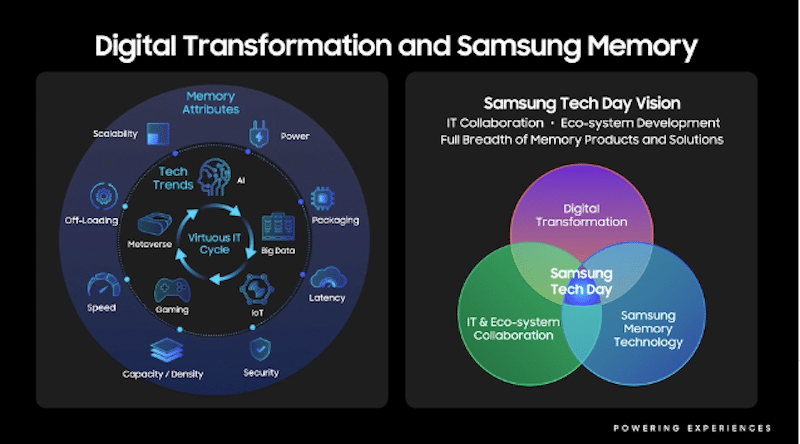
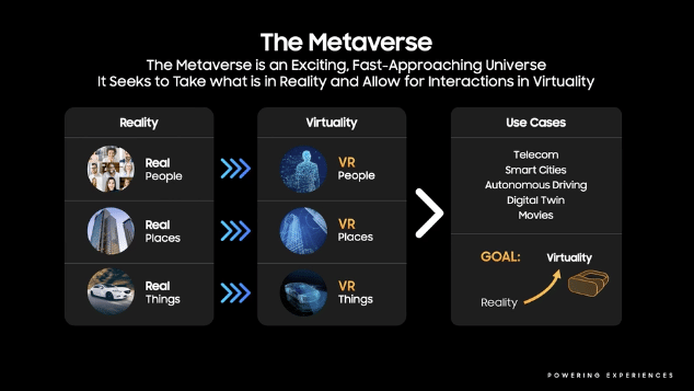
The overall theme was centered on the exponential growth in data and the need to deliver solutions to enable customers to deploy hardware to service technologies such as Big Data, IoT, AI, Computational Storage, and the Metaverse. The pandemic has been driving this growth for almost two years and there doesn’t appear to be any let-up in overall demand.
Computational Storage
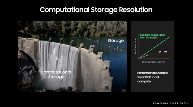
Today, computational storage is important to all enterprise data managers interested in bypassing performance bottlenecks and maximizing the value of their data. Samsung addressed this in a number of presentations during this event validating the technology with a live demo.
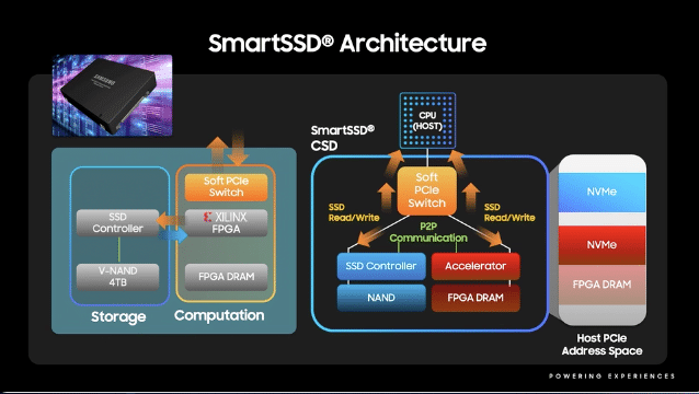
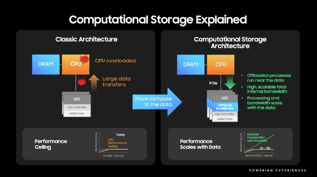
Samsung SmartSSD, a collaboration with Xilinx, was designed to improve workload performance and system efficiency, combines Samsung solid-state storage and a flexible Xilinx FPGA compute engine in a single device. Providing an internal data path between the storage and the FPGA allows data to be transferred much more efficiently for local processing. Local processing with computational storage technology is faster and frees up both host memory bandwidth and I/O interface bandwidth (PCIe lanes). According to Samsung, SmartSSD drives can scale to match the volume of data, without bottlenecks.
The SmartSSD CSD from Samsung is available today and competes in an increasingly crowded field of next-generation computational storage.
The Evolution of Samsung V-NAND
NAND flash memory solutions were designed to store data on a two-dimensional (2D) structure, where chips were scaled and laid onto flat surfaces. But these 2D structures had significant limitations in terms of the amount of data that could be stored.
In 2013 Samsung pioneered its V-NAND (with the ‘V’ standing for vertical) flash memory, a solution that connects its cell layers through pierced holes in vertically-stacked 3D space.
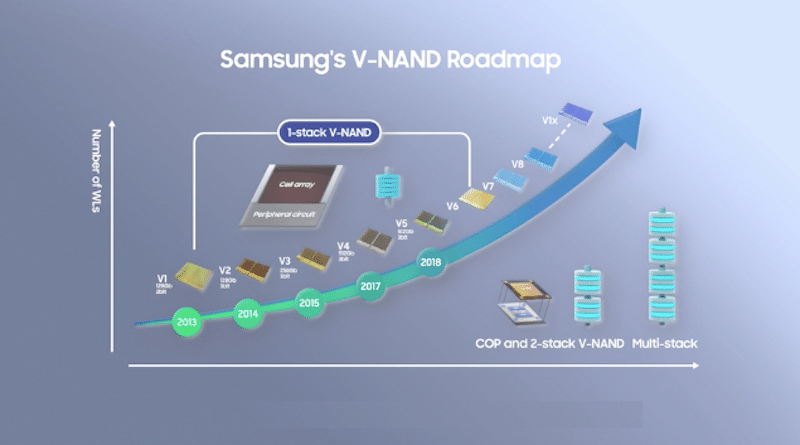
The technical transformation that it enabled can be compared to the experience of people used to living in 1- or 2-story houses moving into high-rise apartments for the first time.
Samsung showcased a consumer solid-state drive (SSD) product based on its 7th generation V-NAND chip, a solution with the smallest cell size yet in the industry. The 7th generation V-NAND solution meets the performance requirements of both the 4thgeneration PCIe interface (PCIe Gen 4) and, later the 5th generation (PCIe Gen 5), thanks to its maximum input-output (I/O) of 2.0 gigabits per second (Gbps).
The 7th generation V-NAND will expand into data center SSDs, reducing power consumption and increasing efficiency by 16% over the 6th generation solution. The company has already secured a working chip of its 8th generation V-NAND solution featuring over 200 layers and plans to introduce it to the market in accordance with consumer demand.

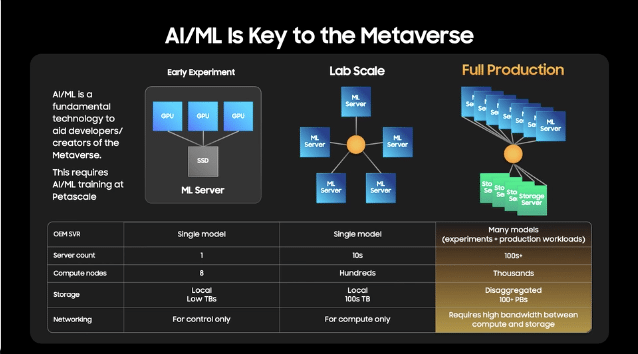
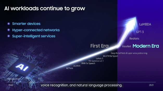
Artificial Intelligence (AI)
Samsung has addressed the overwhelming growth in AI application development and deployment by advancing High-Bandwidth Memory (HBM) and Processing-in-Memory (PIM) development.
Traditional HBM is no longer keeping pace with the rate of innovation happening in the fields of artificial intelligence (AI) and machine learning (ML). This is because AI/ML applications not only process staggering amounts of data but are expected to do it faster and better all the time, which requires increasing amounts of bandwidth.
The concept of processing-in-memory (PIM) technology has been talked about, examined, and tinkered with as a solution to bandwidth limitations for more than 30 years. However, the impetus to solve the technical challenges required to make it viable has not been strong enough. Here’s why:
The problem with PIM technology is that memory and logic integration has always been about making trade-offs of either forfeiting storage density or logic-optimized processing. Consequently, the performance and capability of the resulting PIM device had always underperformed relative to the technical hurdle and cost of the integration.
It’s taken the explosion of AI/ML-based ‘apps’ to spur investment in the development of PIM technology. AI/ML algorithms demand high rates of access to high capacities of data, memory bandwidth and power consumption limiting the performance and capabilities of AI/ML applications. PIM addresses the typical CPU/GPU-memory bandwidth bottleneck, improving AI/ML application performance and capability.
Samsung showcased their new high-bandwidth memory with processing-in-memory (HBM-PIM) technology with integrated high-performance memory, parallel data processing and DRAM on the same piece of silicon. HBM-PIM is based on JEDEC-standard HBM2 specification but enhanced with ‘processor-in-memory’ or PIM architecture. Based on the success of HBM2, Samsung already has plans to include PIM technology in the upcoming HBM3.
Expect to see HBM3 in the 2nd quarter of 2022.
Storage Solutions for a Data-Driven World
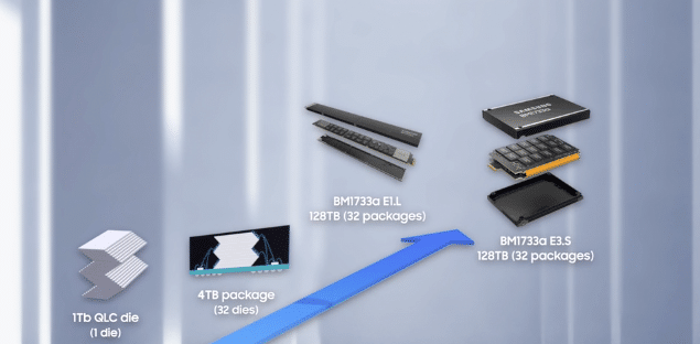
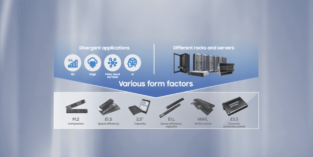
Samsung categorized innovations in storage technology using the five pillar analogy. One of the pillars of storage addresses the constant demand for density. One technology that has gone mainstream in the past year or so is Samsung’s “ruler.” We did a deep dive on the E1.S in September highlighting the pros and cons of the product. You can get some additional background here.
Samsung showed off the new E1.L 128TB SSD during the Data-Driven keynote. This certainly addresses the density requirements for SSD.

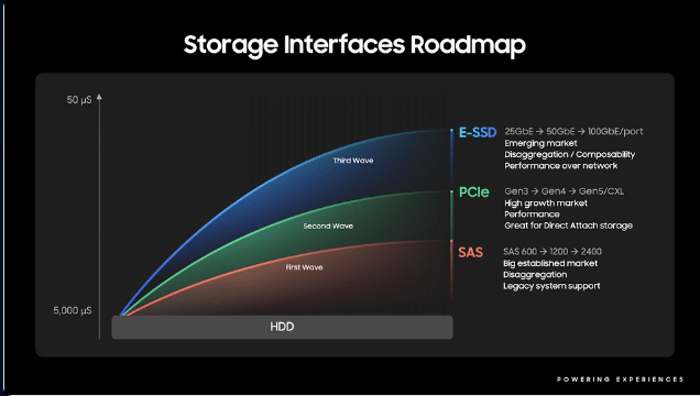
The other pillars were speed, security, interface, and intelligence.
To meet the demands of heavily populated data centers, there is a focus on Ethernet SSDs (E-SSD) reducing the different connection types required for storage. Samsung and NetApp, demoed NVMe-over-Ethernet. The live demo validated the development in E-SSDs showcasing the differences in interface speeds and throughput across the network. Cloud providers have spent billions on building out datacenters based on dense gigabit Ethernet switches. Having the capability to consolidate storage technology interfaces into an Ethernet switch with reduced overall TCO for the cloud provider.
Keeping with the discussion around innovation, Samsung discussed development efforts in PB-SSD and AI-SSD technologies. These are in the early stages of development but certainly on the horizon.
Zoned Namespace SSDs
Samsung provided a demo of its enterprise solid-state drive (SSD) featuring Zoned Namespace (ZNS) technology. Leveraging ZNS, the SSD will maximize available user capacity and offer an extended lifespan in storage server, data center and cloud environments. The PM1731a SSD support ZNS was originally announced in June 2021.
With the release of NVMe 2.0, ZNS has become an acknowledged industry effort to better consume NAND in datacenter workloads; ZNS promises to reduce the TCO of NAND while maintaining a clear separation between the host and the SSD responsibilities. However, one of the remaining challenges for ZNS wide adoption is the changes that application users need to embrace. Specifically, applications that directly implement support for ZNS lose the file system semantics, which poses a limitation for the existing toolchain.
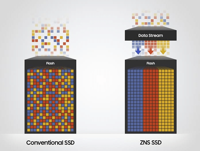
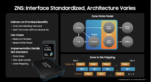 ZNS allows data to be grouped based on their usage and access frequency and stored sequentially in independent zones within an SSD. Without the need to move and rearrange data, ZNS SSDs can significantly reduce the number of write operations, lowering the drive’s write amplification factor (WAF) — the number of actual writes performed by the drive compared to writes initially instructed by the host system. The closer the WAF is to one, the more efficient the SSD and the longer it will last.
 Although ZNS adoption is gaining traction, there is still a way to go before all vendors begin supporting this technology. Currently Samsung and Western Digital have embraced ZNS.
Wrap-up
These are just a few of the topics addressed during Samsung’s Tech Day event. Although it was virtual, the content was solid, with relevant demos and support from partners. Several universities participated in delivering demos as well. If you are interested in learning more, the original link to the event is here – Samsung Tech Day.
Samsung PM1743 Launched 12/23/21


 Amazon