

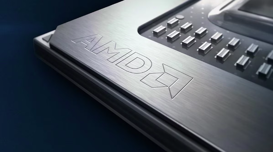
AMD announced that its next-generation EPYC processor, codenamed “Venice,” has entered production on TSMC’s 2nm process in Taiwan. The company also plans to expand manufacturing at TSMC’s Arizona facility, signaling a broader strategy to diversify its advanced-node capacity and scale supply for cloud and AI deployments.
“Venice” is positioned as the first HPC-class processor to ramp on TSMC’s 2nm node. The transition to 2nm is expected to improve performance per watt and transistor density, both of which are critical for data center operators facing power and cooling constraints. AMD framed this milestone as part of its ongoing EPYC roadmap execution, with a focus on enabling higher core density, improved efficiency, and tighter integration across compute subsystems.
Venice is also expected to introduce the new SP7 socket, a physically larger platform than the outgoing SP5 that is designed to accommodate higher power delivery, additional memory channels, and expanded I/O bandwidth to support significantly higher core counts per socket.
CPU Role Expands with AI and Data Center Orchestration
AMD emphasized that CPUs remain central to modern AI infrastructure, even as accelerators handle model training and inference. In production environments, CPUs orchestrate data pipelines, manage storage and networking stacks, enforce security, and coordinate distributed workloads. As AI evolves toward more complex agentic workflows, these responsibilities expand, placing additional demands on CPU performance, memory bandwidth, and I/O.
The “Venice” ramp aligns with this shift. By leveraging the 2nm process, AMD is targeting efficiency and throughput gains that support large-scale AI clusters and traditional enterprise and HPC workloads. The company continues to see momentum in EPYC adoption across hyperscale and enterprise environments, where consolidation and energy efficiency remain key buying criteria.
Manufacturing Strategy and TSMC Partnership
Initial production in Taiwan will be followed by a planned ramp-up at TSMC’s Arizona fab, reflecting AMD’s effort to balance leading-edge manufacturing with geographic resilience. This approach is increasingly relevant to enterprise buyers, given supply chain and regulatory considerations in data center infrastructure sourcing.
AMD and TSMC continue to collaborate on process and packaging technologies. In addition to the 2nm node, AMD is leveraging advanced packaging technologies, including SoIC-X and CoWoS-L, across its broader data center and AI portfolio. These technologies enable higher-bandwidth interconnects and tighter integration among compute dies, memory, and accelerators, which are now standard requirements for AI-optimized platforms.
Roadmap Outlook with “Verano”
Looking ahead, AMD plans to extend its use of TSMC’s 2nm technology with “Verano,” identified as a 6th Gen EPYC processor. Verano is expected to deliver improvements in performance per dollar and per watt, with design optimizations for cloud and AI workloads. AMD also indicated support for advanced memory technologies, including LPDDR, which could improve power efficiency and memory bandwidth in scale-out deployments.
Verano is expected to adopt the new SP8 socket, which succeeds today’s SP6 and targets a more conventional power envelope. SP8 is positioned for mainstream and entry-level server deployments, retaining a more familiar thermal profile while still benefiting from the move to 2nm, next-generation I/O, and updated memory support. The two-socket strategy gives AMD broader coverage across the data center stack, with SP7 addressing maximum performance requirements and SP8 supporting power-conscious and cost-sensitive footprints across general-purpose enterprise and edge infrastructure.
The Venice ramp and the Verano roadmap underscore AMD’s continued investment in CPU innovation as a foundational layer of AI infrastructure. While GPUs and accelerators dominate headlines, the CPU remains a critical control plane for data movement and system orchestration. Advancements in process and packaging will directly shape how efficiently next-generation data centers scale compute, storage, and networking resources.
With Venice entering production, Verano on the horizon, and two new sockets reshaping the platform landscape, the processor segment is set for a particularly active stretch. We are looking forward to what AMD has in store at AMD Advancing AI 2026, where the next phase of this roadmap is expected to come into sharper focus.


 Amazon