

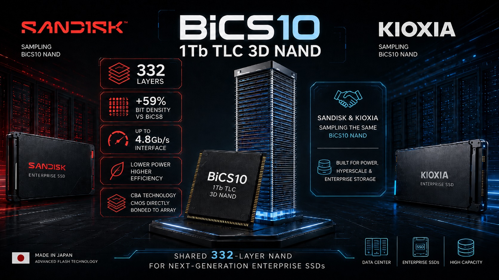
Sandisk and Kioxia have both begun sampling BiCS10 1Tb TLC 3D NAND, the 10th generation of the BiCS flash memory the two companies jointly develop and manufacture. The announcements land in parallel because the technology is shared: Sandisk is framing it around higher density, faster interfaces, and better power efficiency for data-intensive workloads, while Kioxia is aiming its version squarely at enterprise and data center SSDs built to meet the growing demand of AI storage. It is the same 332-layer NAND from the same joint venture, announced from both sides.
A 332-Layer Jump in Density
The headline change is all about the layers. BiCS10 stacks 332 layers and, combined with advanced lateral scaling and improved floor-plan efficiency, reaches an industry-leading 1Tb TLC memory density greater than 29 Gb/mm2. Against the 8th-generation BiCS8 node currently in mass production, that works out to a 59% improvement in bit density. Higher bit density is the number that matters most to buyers, since it is what lowers cost per bit and lets drive makers pull more capacity out of the same die area. At 332 layers, BiCS10 sits at the leading edge of the 3D NAND stack race, in the same class as SK hynix’s 321-layer generation and a clear step beyond the 276-layer nodes that defined the previous wave.
Faster Interface, Lower Power
BiCS10 TLC supports a NAND interface speed of up to 4.8 Gb/s, a 33% improvement over the 8th-generation flash in mass production, giving controller makers the NAND-side bandwidth that coming PCIe Gen6-class SSDs will need. Power efficiency also improves, though the two partners quantify it differently. Sandisk cites a 10% reduction in data input power and a 34% reduction in data output power versus BiCS8. Kioxia frames the gains as 18% and 30% improvements in write and read power efficiency. Either way, the direction is the same, and the benefit is most meaningful in dense enterprise and data center deployments where NAND power adds up across thousands of drives.
Built on CBA, Made at Kitakami
Both companies continue to build on CMOS directly Bonded to Array (CBA) technology, in which the CMOS logic and the memory array are fabricated on separate wafers and then bonded together with wafer-to-wafer alignment. First adopted at the 8th generation, CBA is paired here with On-Pitch Select Gate Drain (OPS) technology, and BiCS10 extends that foundation with a taller, denser array. Kioxia says the 10th-generation devices will be manufactured with state-of-the-art equipment at its Kitakami Plant Fab2 in Iwate Prefecture, Japan.
Kioxia also positioned BiCS10 within what it calls a dual-axis strategy, advancing two product lines at once: its 9th-generation technology for high performance at a lower investment cost, and its 10th-generation technology, which relies on advanced layer stacking for massive capacity and higher performance. For Sandisk, the milestone is also an early marker as a standalone company following its 2025 separation from Western Digital, with BiCS10 among its first next-generation NAND announcements under the independent Sandisk banner.
Availability
BiCS10 1Tb TLC is in the sampling stage, meaning the devices are going to partners for functional evaluation before broader availability, and sample specifications may differ from mass production. Sandisk has not shared a mass-production timeline or named the first commercial products, while Kioxia has only confirmed production is planned at its Kitakami Plant Fab2. Given both companies’ point BiCS10 at enterprise, data center, and AI storage, the first drives to use it will most likely be Gen6 high-capacity enterprise and hyperscale SSDs.


 Amazon