

The NVIDIA DGX Spark represents a watershed moment in accessible AI infrastructure. In 2017, the landmark “Attention is All You Need” paper that introduced the Transformer architecture relied on an eight-GPU P100 server configuration, consuming tens of kilowatt-hours and occupying significant data center real estate. Today, the DGX Spark delivers superior computational performance in a compact 240-watt desktop form factor. This dramatic evolution in power efficiency and form factor compression makes formerly datacenter-exclusive AI capabilities accessible to individual researchers, small teams, and distributed development organizations.
What distinguishes Spark from previous desktop AI solutions is its comprehensive approach to the full development lifecycle. Rather than forcing compromises between experimentation, fine-tuning, and deployment, Spark provides genuine capability across all phases. The 128 GB unified memory architecture enables full parameter fine-tuning of models that would require cloud resources on conventional workstations, while delivering hundreds of tokens per second throughput suitable for batch inference workloads, including synthetic data generation. The inclusion of ConnectX-7 networking with 200Gb fabric capability means organizations can cluster multiple Spark systems for even larger model exploration, though as we’ll demonstrate, even a single unit proves remarkably capable.
Key Takeaways
Datacenter power in a desktop: GB10 Grace Blackwell in a 1.13-liter, 240W box, priced at $3,999, delivering up to 1 petaFLOP FP4 sparse performance.
Memory that changes workflows: 128GB unified memory enables full-parameter fine-tuning of 8B models locally and high-throughput inference. In testing we saw Llama 3.1 8B FP4 reach ~924 tok/s at 128 concurrency, and Qwen3 Coder 30B-A3B FP8 hit ~483 tok/s at batch 64.
Ready to scale and attach fast storage: Integrated ConnectX-7 provides 200G fabric for clustering or NVMe-oF. The internal 2242 Gen5 NVMe is convenient but limited for heavy I/O, so external NVMe-oF over RDMA is the better path for sustained throughput.
Day-one software maturity: Ships with DGX OS, CUDA, cuDNN, TensorRT, AI Workbench, containers, and workflow playbooks so teams can run real workloads immediately.
Proven real-world performance: MAMF measured ~99.8 TFLOPs BF16 and ~207.7 TFLOPs FP8. GDSIO reads peaked ~11.4 GiB/s internally, with higher ceiling expected over the 200G fabric.
What is DGX Spark, and Who Should Consider It?
The NVIDIA DGX Spark is fundamentally a complete AI development platform rather than simply a GPU component. At its core sits the GB10 Grace Blackwell Superchip, which integrates a Blackwell architecture GPU featuring fifth-generation Tensor Cores with a 20-core Arm CPU (10× Cortex-X925 + 10× Cortex-A725) connected via NVLink-C2C. This coherent interconnect architecture, according to NVIDIA, enables up to 5× higher bandwidth compared to PCIe Gen 5, creating a unified computational fabric rather than discrete processing domains.
To get users started, NVIDIA ships DGX OS built on Ubuntu Desktop with the complete AI software stack pre-configured, including CUDA, cuDNN, TensorRT, NVIDIA Container Runtime, and AI Workbench, eliminating the typical driver challenges and environment configuration overhead that plagues custom workstation builds. The system offers flexible deployment paradigms: attach peripherals and use it as a compact workstation with the full Ubuntu desktop experience, or deploy it as a headless network appliance accessible via NVIDIA Sync, which provides seamless integration with JupyterLab, VS Code, Cursor IDE, and SSH terminals.
This is purpose-built infrastructure for AI practitioners, researchers fine-tuning language models, data scientists accelerating RAPIDS workflows, developers implementing agentic systems, or teams experimenting with architectures with ablative models at a small scale. Spark targets professionals who need serious AI computational capability without datacenter complexity.
NVIDIA DGX Spark Technical Specifications
| Specification | Details |
|---|---|
| Architecture | |
| GPU | NVIDIA Blackwell Architecture |
| CPU | 20-core Arm (10x Cortex-X925 + 10x Cortex-A725) |
| Tensor Cores | 5th Generation |
| RT Cores | 4th Generation |
| NVENC / NVDEC | 1× / 1× |
| Memory | |
| System Memory | 128 GB LPDDR5X (Unified System Memory) |
| Memory Interface | 256-bit |
| Memory Bandwidth | 273 GB/s |
| Performance | |
| FP4 | up to 1 petaFLOP (with Sparsity) |
| Storage | |
| Storage | 1 TB or 4 TB NVMe M.2 (Self-encrypted) |
| Connectivity | |
| USB | 4× Type-C USB 3.2 Gen 2×2 (20Gbps) |
| Ethernet | 1× 10GbE RJ-45 |
| NIC | ConnectX-7 Smart NIC – 2x 200G QSFP (Allows for a maximum of 200G bandwidth) |
| Wireless | Wi-Fi 7, Bluetooth 5.3 |
| Audio Output | HDMI Multichannel Audio Output |
| Display Connectors | 1× HDMI 2.1a |
| Mechanical | |
| Dimensions | 150 × 150 × 50.5 mm (5.9 × 5.9 × 1.98″) |
| Weight | 1.2 kg |
| Power Consumption | 240 W |
NVIDIA DGX Spark Design & Build
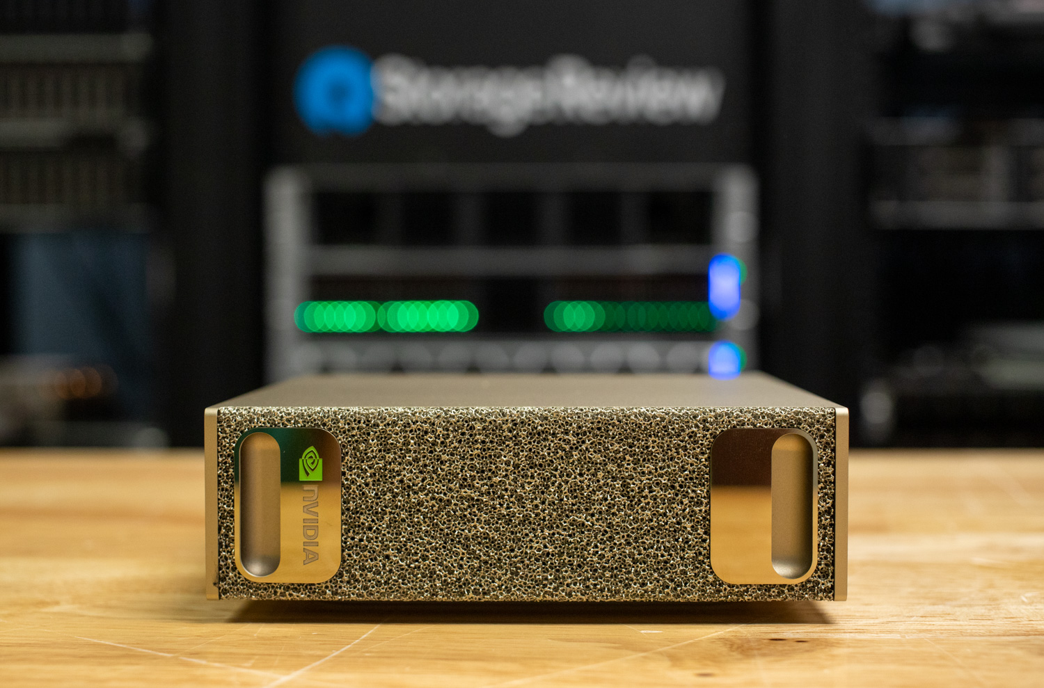
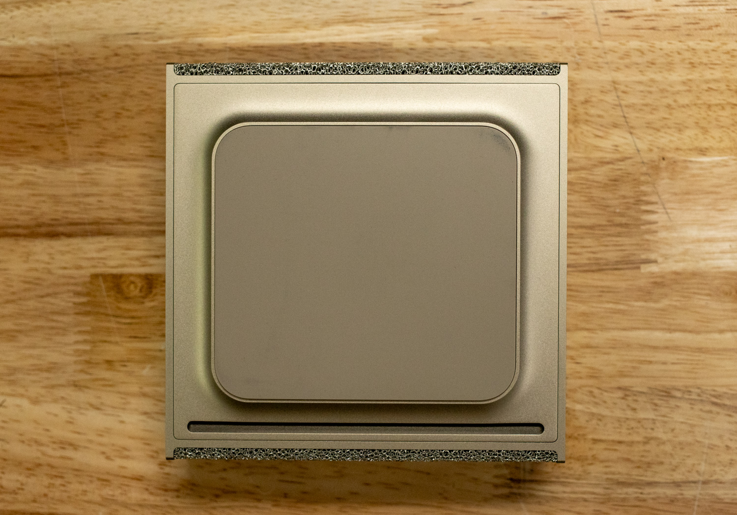
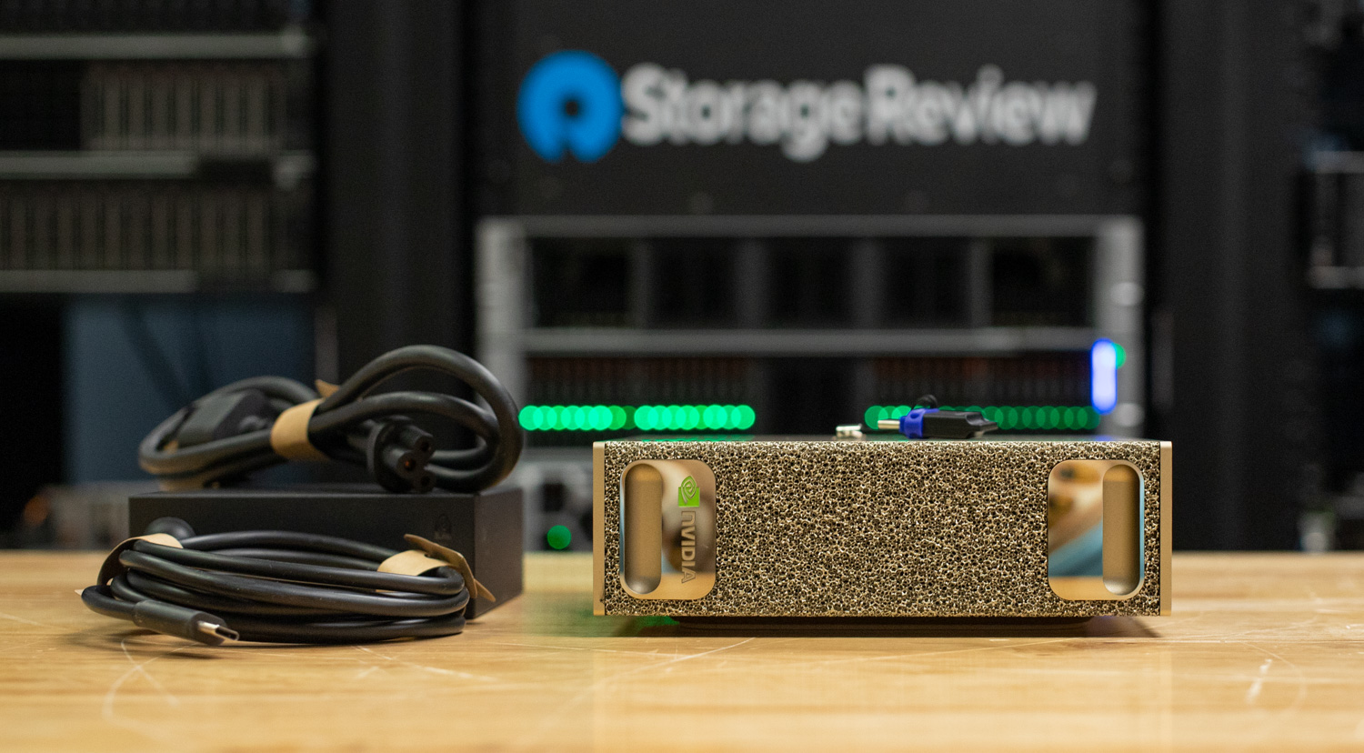
The NVIDIA DGX Spark continues NVIDIA’s unmistakable industrial design language, featuring a compact chassis that mirrors the look and feel of its larger DGX systems. The front panel features miniature hand-hold cutouts, a nod to the original full-sized DGX units’ handles, and a gold-speckled metallic finish that delivers a refined, premium texture, accented by NVIDIA’s iconic green logo badge.
Physically, the DGX Spark measures 5.9 × 5.9 × 1.98 inches (150 × 150 × 50.5 mm) and weighs 2.6 pounds (1.2 kg), giving it a total internal volume of 1.13 liters. This places it firmly within the 1-liter small-form-factor PC class. Despite its minimal footprint, the system feels dense and robust thanks to an all-metal alloy shell that also serves as a passive heat spreader, maintaining focus on both form and function.
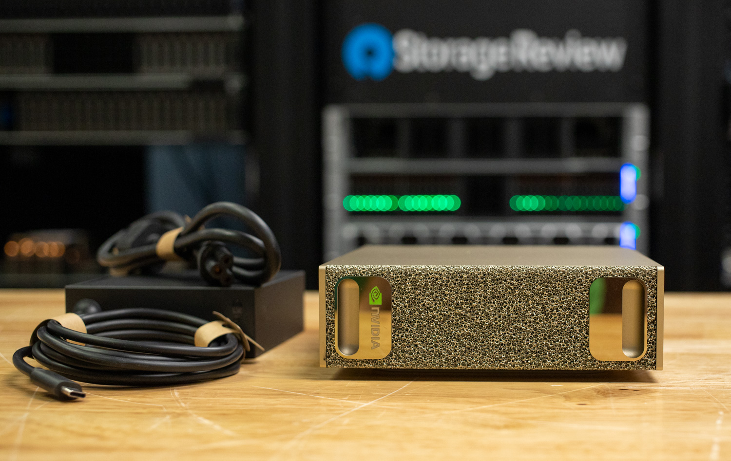
Power is provided by a 240 W USB-C external power brick, seen beside the main unit in the image. The brick is compact and well-built, using a standard C5 (cloverleaf) connector for AC input and matching the DGX Spark’s clean, efficient design.
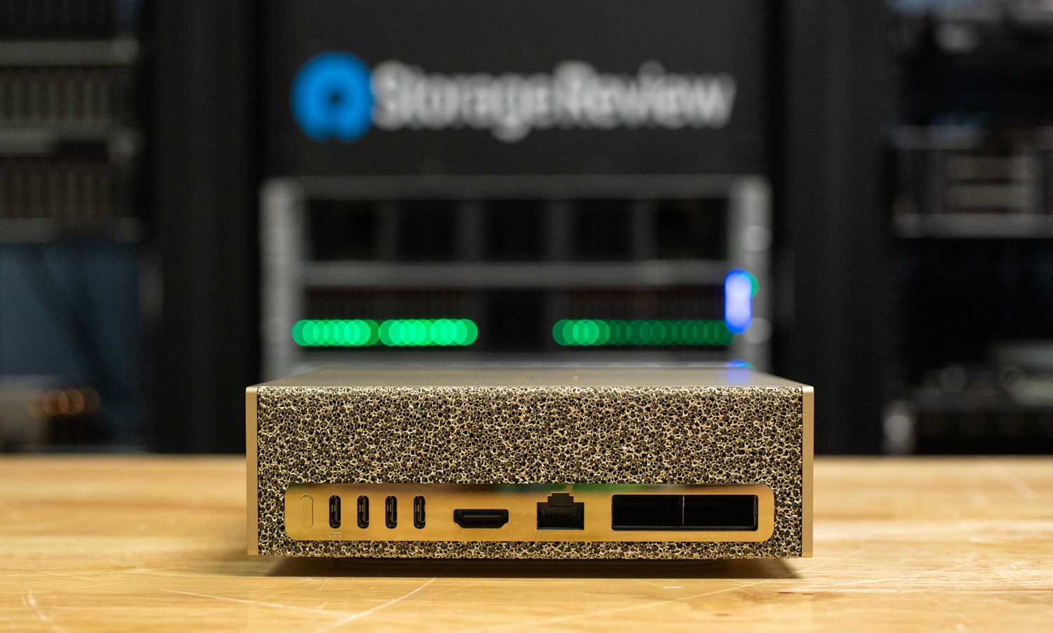
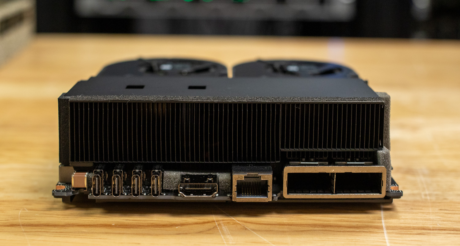
Turning to the rear, the DGX Spark carries over the same gold-speckled textured finish seen on the front, maintaining a cohesive design throughout the chassis. Starting from the left, the power button sits beside four USB-C ports, one of which provides Power Delivery for the unit. These are followed by a single HDMI 2.1a output, a 10 GbE RJ-45 port, and what makes this unit interesting is the dual 200 GbE QSFP56 interfaces driven by an integrated NVIDIA ConnectX-7 SmartNIC.
At first glance, you might deduce that the Spark allows for 400G of connectivity; unfortunately, due to PCIe limitations, the Spark is only able to provide 200G of connectivity. Wanting to know more, we dug deeper into the topology of the Spark:
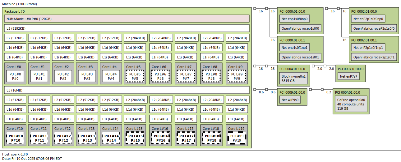
Using lstopo, we observe the two interconnects from the CX7 NIC. Electrically, the CX7 is connected via two Gen5 x4 links. Within the OS, these connections appear as four interfaces, each supporting a maximum bandwidth of 200G. Due to limited test time, we were unable to discover all networking quirks of this platform outside of our NVMe-oF tests, which are detailed later in the article. However, we plan to explore this platform further and will release future articles that dive deeper into its capabilities, like clustering multiple sparks together for a mini cluster.
Looking into other connected devices, next up is the tiny 2242 form factor M.2 SSD connected with Gen5 x4, followed by the Realtek RJ45 10GbE controller connected with PCIe Gen4 x1 link, and the MediaTek Wi-Fi Controller connected with a PCIe Gen3 x1 link.
Diving into the CPU, the Spark contains a 20-core Arm processor with a heterogeneous big little architecture, similar to Intel’s latest processors, consisting of 10 Cortex-A725 efficiency cores and 10 Cortex-X925 performance cores split across two L3 cache clusters. The first cluster (8MB L3) contains CPUs 0-4 (Cortex-A725, max 2808 MHz) and CPUs 5-9 (Cortex-X925, max 3900 MHz), while the second cluster (16MB L3) contains CPUs 10-14 (Cortex-A725, max 2860 MHz) and CPUs 15-19 (Cortex-X925, max 3978-4004 MHz). Each core has private 64KB L1 data and 64KB L1 instruction caches, but the L2 cache differs significantly by core type: the efficiency Cortex-A725 cores have 512KB L2 caches, while the performance Cortex-X925 cores have substantially larger 2MB L2 caches (4× larger). The fastest cores are CPUs 15-19, which benefit from both the larger 16MB L3 cache and higher frequencies, with CPU 19 being the peak performance core at 4004 MHz. These different power/frequency levels are signified by the dashed lines on the core on the topology shown above.
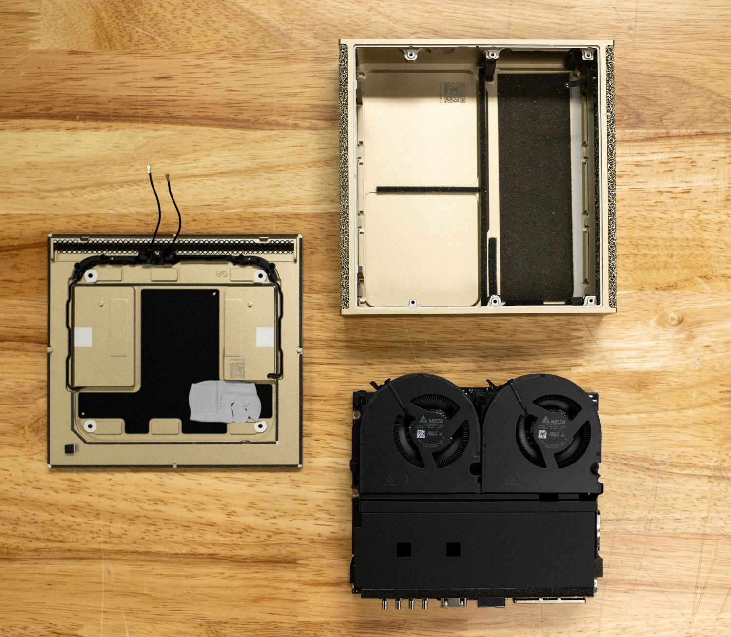
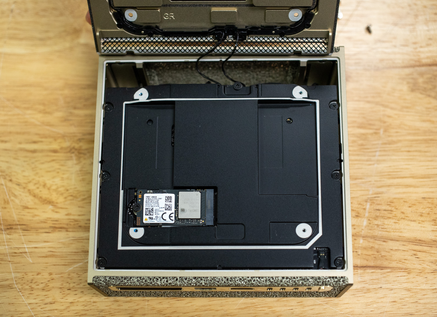
Zooming back out, we flip the DGX Spark over; the only visible plastic component is the base cover, which attaches magnetically to the bottom of the chassis. This design keeps the exterior clean while allowing for quick access to the internals. Once the magnetic base is removed, four screws are exposed, granting access to the main internal compartment.
Inside, we can see antenna wiring routed toward the top section of the unit, confirming the inclusion of Wi-Fi 7 and Bluetooth 5.3 connectivity. This provides flexible network options, particularly useful for mobile or lab deployments where wired access may not be available.
Also visible is the unit’s storage solution, a PCIe Gen5 2242 M.2 SSD, a less-common form factor for such high-performance hardware. The configuration shown here includes a 4TB Samsung NVMe drive in our configuration.
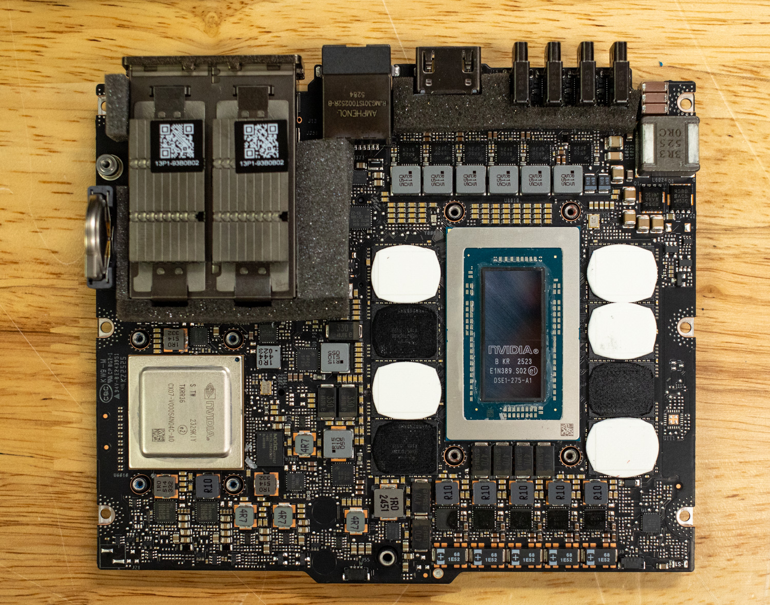
Diving deeper into the DGX Spark reveals the heart of the system, the NVIDIA Grace Blackwell’s GB10 Superchip. Flanking the GB10 Superchip are the 8 soldered LPDDR5X unified system memory delivering 273 GB/s of bandwidth, ensuring fast data access across both CPU and GPU operations.
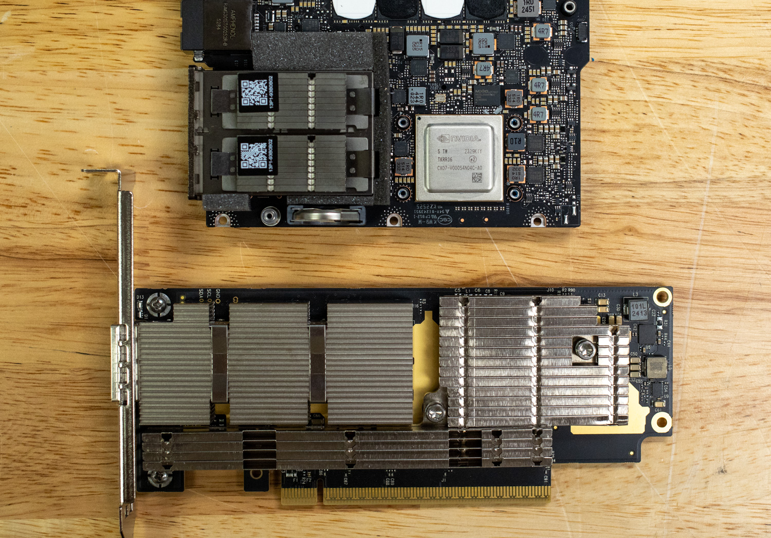
Right next to the chip is the CX7 NIC, which, as previously mentioned, provides 200G of connectivity. This allows users to connect the Spark to high-speed storage or even cluster multiple instances of the Spark together. NVIDIA has validated and sells a cluster of 2 Sparks that can be directly connected to support even bigger AI models.
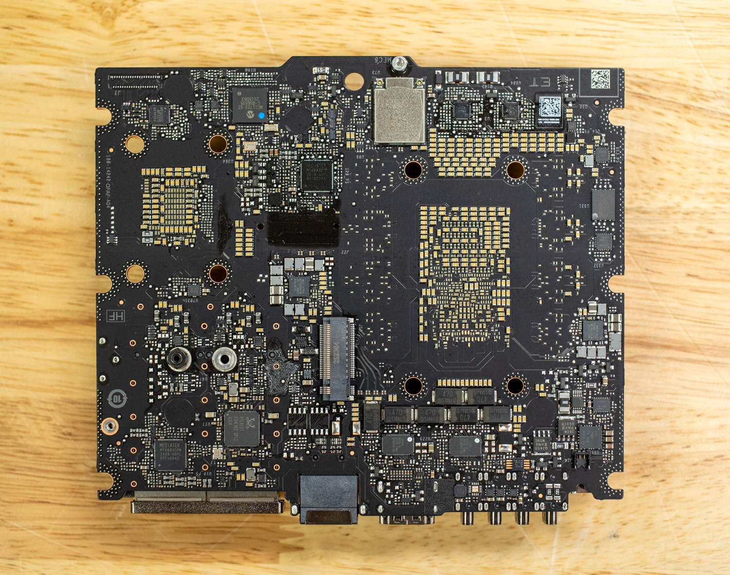
Finally, flipping the board over reveals all the PCIe connectivity, including the PCIe Gen5 x4 2242 M.2 SSD and the PCIe Gen3x1 MediaTek Wi-Fi adapter.
Where Spark Becomes Indispensable: The Modern AI Development Appliance
The DGX Spark proves particularly compelling across several distinct professional contexts, each benefiting from its unique combination of unified memory, compact form factor, and comprehensive software integration.
Data Science Acceleration: From Pandas to Production
For data scientists, the NVIDIA DGX Spark represents a big improvement in workflow velocity and experience. The ConnectX-7 networking delivering 200 Gbps bandwidth, combined with CUDA X accelerated libraries, transforms data preprocessing. AI and Data Science are built on the foundation of good data in, good data out. Traditionally, the most time-consuming phase of any conventional ML project is data cleaning and feature extraction. Conventional workflows typically involve loading datasets into tools like pandas and performing transformations on CPU cores, which is generally slow. Manual exploration and feature engineering can also be a significant blocker. Spark enables end-to-end GPU acceleration through RAPIDS.
A typical enterprise data science scenario involves feature engineering on datasets in the 40-80GB range: joining multiple tables, computing aggregations across temporal windows, handling categorical encoding, and normalizing distributions. On CPU infrastructure, this preprocessing might consume hours. With RAPIDS cuDF loading the entire dataset into Spark’s 128 GB unified memory, these operations complete in minutes at 10× or higher acceleration. The subsequent model training benefits equally whether classical ML with cuML or deep learning with PyTorch, eliminating the traditional bottleneck where data scientists wait on infrastructure rather than iterating on hypotheses.
Synthetic Data Generation: Robotics and Simulation
The inclusion of fourth-generation RT Cores positions Spark uniquely for an emerging workflow: synthetic data generation for world model training. Training robust manipulation policies traditionally requires tens of thousands of real-world demonstrations, prohibitively expensive and time-consuming. Photorealistic simulation in platforms like Isaac Sim or Omniverse provides an alternative, but rendering ray-traced imagery with physically accurate lighting, reflections, and materials historically demanded expensive workstation GPUs like NVIDIA’s L40S and RTX 6000 Ada.
Source: NVIDIA
Spark consolidates this workflow. RT Cores enable OpenUSD workloads to handle synthetic data generation, while Tensor Cores are used for AI inference in a blueprint/workflow. Previously, organizations might deploy multiple machines for rendering and a separate inference-optimized server. Now, this is achievable in a single 240W appliance. For robotics startups, university labs, or automotive manufacturers exploring autonomous manipulation, this integration significantly reduces development timelines and capital expenditure.
We have previously explored similar synthetic data generation pipelines using dedicated L40S rendering systems paired with H100 for inference in our earlier coverage of NVIDIA L40S. The GB10’s architectural consolidation of these capabilities into a unified development appliance represents a compelling evolution of this workflow. We plan to conduct additional testing of Spark’s RT Core performance against these discrete configurations in forthcoming analysis, examining rendering and other workloads for representative robotics manipulation scenarios.
The Vibe Coding Revolution
Andrej Karpathy, formerly Tesla’s AI director and OpenAI’s founding member, coined the term “vibe coding” to describe an emerging approach to rapid software development with AI assistance. Rather than meticulously writing code line-by-line, vibe coding leverages LLMs as interactive pair programmers: describe functionality in natural language, generate implementation scaffolding, iterate through conversational refinement, and rapidly prototype features. This workflow transforms coding from deliberate construction to guided conversation with an AI that understands context, APIs, and architectural patterns, enabling individual developers to build remarkably sophisticated systems at unprecedented velocity.
The scale of AI-assisted coding adoption is evidenced by OpenRouter’s usage rankings, where coding-focused models consistently dominate inference volume. Technical professionals, the primary vibe coding demographic, typically operate as power users, running multiple coding agents in parallel across different contexts. And as open-weight models increasingly match proprietary alternatives on key benchmarks, developers are exploring local inference deployments to eliminate rate limiting, ensure availability during critical development windows, and maintain code confidentiality for proprietary projects.
The r/LocalLLaMA community showcases truly impressive custom builds, ranging from multi-GPU workstations to duct-taped-together servers running local models, distributed inference across consumer hardware, and elaborate cooling solutions that enable sustained high-throughput generation. However, these configurations present significant barriers: capital expenditure often exceeding tens of thousands of dollars, substantial power consumption, thermal management challenges requiring dedicated spaces rather than standard office environments, and considerable technical expertise for configuration, optimization, and troubleshooting.
Spark fundamentally alters this value proposition. At $3,999 with 128 GB unified memory, it delivers impressive model inference performance in a quiet, compact, power-efficient appliance drawing just 240W. Users seeking to establish local coding assistant infrastructure no longer require elaborate homelabs that consume kilowatt-hours and generate substantial heat output. The validated appliance approach with pre-configured DGX OS eliminates the configuration complexity that previously restricted local LLM deployment to users with deep Linux and CUDA expertise.
Beyond eliminating infrastructure friction, Spark addresses critical concerns around code privacy and model customization. Cloud-based coding assistants necessarily transmit source code to remote servers, which is a non-starter for organizations handling proprietary algorithms, security-critical infrastructure, or regulated data. Local inference on Spark ensures code never leaves the development environment. Furthermore, the 128 GB memory capacity enables full parameter fine-tuning of coding models, allowing experienced developers to specialize models on internal codebases. This capability is particularly valuable for organizations with domain-specific languages, custom frameworks, or architectural patterns that are insufficiently represented in public training data.
Fine-Tuning with NVIDIA NeMo on DGX Spark
The DGX Spark’s 128 GB unified memory enables full parameter fine-tuning of 8B models that traditionally required expensive multi-GPU cloud setups. Full fine-tuning Qwen3 8B with standard Adam optimization requires approximately 132 GB (16 GB model weights, 96 GB optimizer states, 16 GB gradients, plus activations), exceeding dual H100 80 GB configurations. Using memory-efficient 8-bit Adam reduces requirements to around 70 GB, depending on batch size, comfortably fitting within Spark’s memory pool. This matters because full fine-tuning delivers 4-6% better accuracy than LoRA on complex reasoning tasks. Where cloud-based 2× H100 80 GB setups cost about $5 an hour with distributed training complexity, Spark provides single-system training at a one-time $3,999 investment.
NVIDIA NeMo Automodel eliminates enterprise training framework friction by providing Day-0 support for any Hugging Face model without checkpoint conversion. Load Qwen3 8B directly from HuggingFace Hub and configure fine-tuning through YAML files specifying dataset sources, optimizer settings, and LoRA targets. NeMo automates distributed checkpointing with safetensors compatibility, implements fused CUDA kernels for 2-5× speedups, and handles gradient accumulation.
Image Generation with Comfy UI
ComfyUI provides a node-based graphical interface that transforms Stable Diffusion and related diffusion models into highly customizable creative pipelines. Unlike traditional web-based interfaces that abstract complexity behind simplified parameter sliders, ComfyUI employs a visual graph architecture where users construct workflows by connecting discrete functional nodes, each representing specific operations such as model loading, prompt encoding, latent diffusion sampling, VAE decoding, or upscaling transformations. This modular design enables granular control over the entire generation pipeline, making every computational step transparent and adjustable. It also allows users to chain multiple models, implement custom sampling schedules, or integrate advanced techniques like ControlNet guidance, which would be impossible in simplified interfaces.
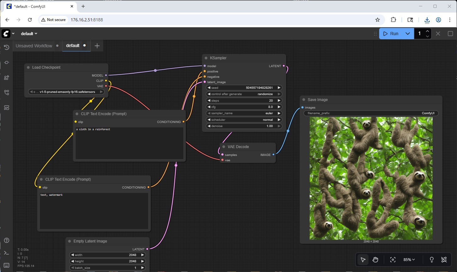
On DGX Spark, ComfyUI leverages the Blackwell GPU’s Tensor Cores for accelerated diffusion sampling, typically completing generations in 15-30 seconds depending on sampling complexity. The 128GB unified memory architecture proves particularly advantageous, maintaining multiple checkpoint models, LoRA adapters, and VAE decoders in memory concurrently, eliminating the reload overhead that plagues VRAM-constrained systems. Users can generate effectively unlimited AI artwork locally, free from API rate limits, cloud costs per generation, and privacy concerns associated with proprietary creative workflows. The workflow persistence model adds operational value: complete pipelines serialize to JSON files that can be version-controlled, shared across teams, or embedded directly into generated images as metadata, enabling reproducibility critical for organizations building synthetic dataset pipelines or maintaining consistent artistic styles across generated assets.
NVIDIA DGX Spark Performance Testing
vLLM Online Serving – LLM Inference Test
vLLM is the most popular high-throughput inference and serving engine for LLMs. The vLLM online serving benchmark is a performance evaluation tool designed to measure the real-world serving capabilities of this inference engine when handling concurrent requests. It simulates production workloads by sending requests to a running vLLM server with configurable parameters, such as request rate, input/output lengths, and number of concurrent clients. The benchmark measures key metrics, including throughput, i.e., tokens per second, time to first token, and time per output token, helping users understand how vLLM performs under different load conditions.
We tested the inference performance across a comprehensive suite of models representing the most popular architectures and model types in production deployments today.
Mixture of Experts Models
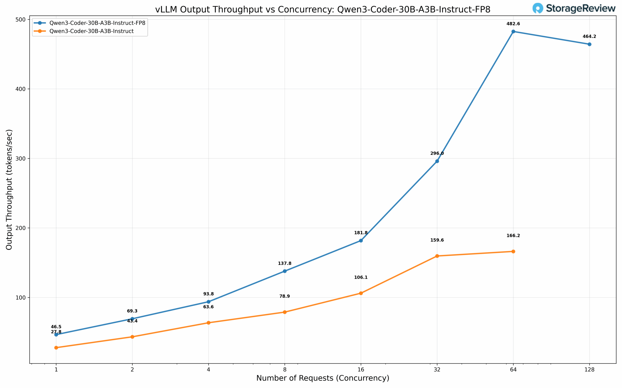
We evaluated the Qwen3 Coder 30B-A3B, one of the most popular coding models for local inference deployments. This sparse architecture maintains a full model size of 30B parameters at BF16 precision while activating only 3B parameters per generated token. We benchmarked both the stock model and an FP8 quantized variant from Qwen. The FP8 quantized model demonstrates substantial performance gains: achieving 46.5 tok/s at concurrency 1, scaling to an impressive 482.6 tok/s at batch size 64. The stock BF16 model delivers 27.8 tok/s at concurrency 1, reaching 166.2 tok/s at batch size 64, a nearly 3x performance differential.
Dense Models
Dense models represent the conventional LLM architecture where all parameters and activations are engaged during inference, resulting in more computationally intensive processing compared to their sparse counterparts. To comprehensively evaluate performance characteristics across model scales and quantization strategies, we benchmarked five dense model configurations.
Our test suite included Mistral Small 3.1 24B from Mistral AI at BF16 precision, alongside a Mistral Small 3.1 24B FP8 dynamically quantized variant from RedHat AI. Dynamic quantization employs selective weight quantization techniques to optimize the performance-accuracy tradeoff, strategically reducing precision while minimizing model degradation. We complemented these larger dense models with Meta Llama 3.1 8B evaluations across three precision formats: the stock BF16 configuration, plus FP8 and FP4 quantized versions from NVIDIA. This model selection strategy enables direct performance comparison across model scales while isolating the impact of progressive quantization on inference throughput.
Performance Analysis: Large Dense Models
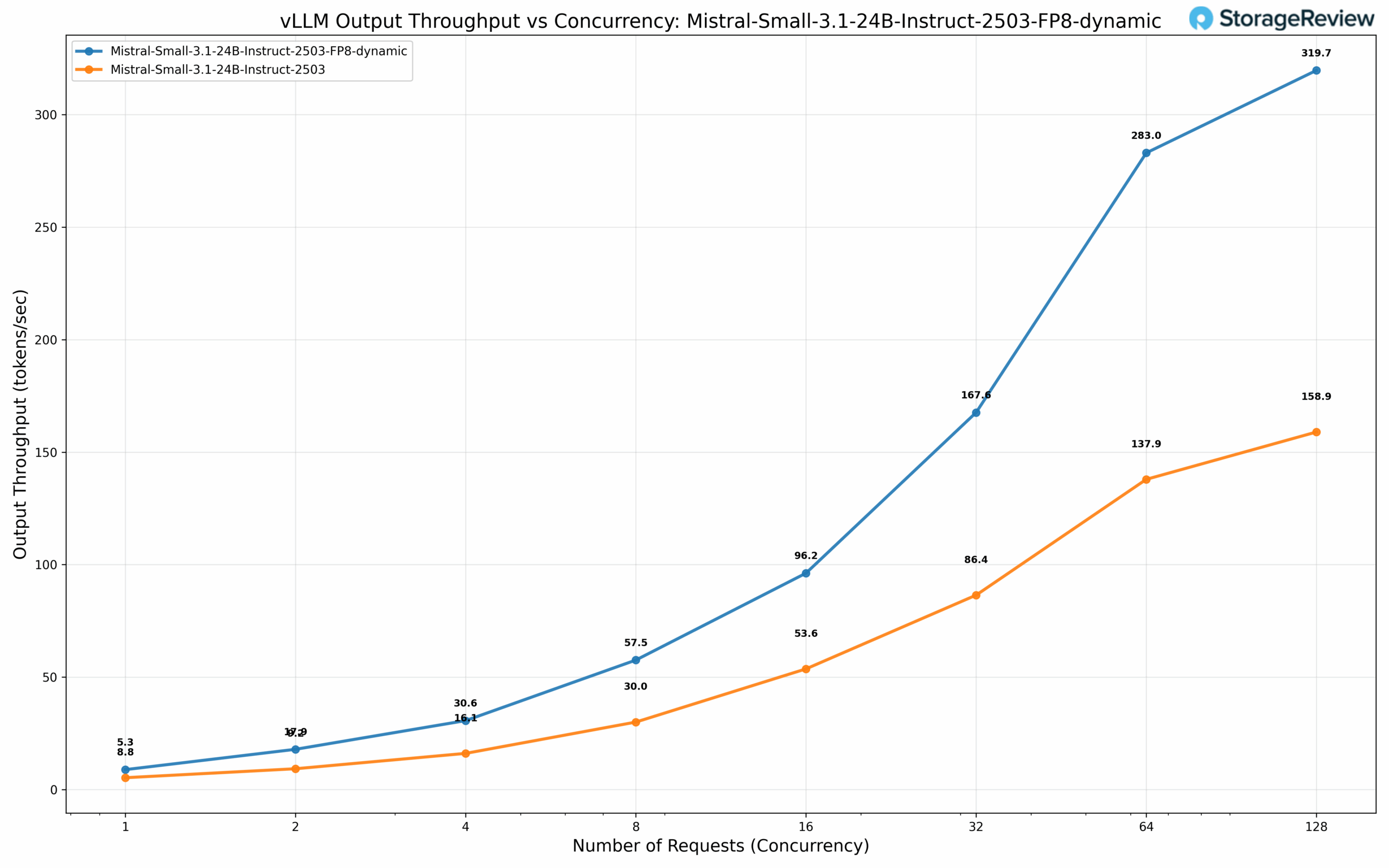
The Mistral Small 3.1 24B at BF16 precision exhibits baseline throughput of 5.3 tok/s at concurrency 1, scaling to a substantial 158.9 tok/s at 128 concurrent requests. The FP8 dynamically quantized variant demonstrates modest gains at lower concurrency with 8.8 tok/s, but delivers a compelling 2x performance multiplier at scale, achieving 319.7 tok/s at 128 concurrency—underscoring the effectiveness of dynamic quantization for high-throughput serving scenarios.
Performance Analysis: Compact Dense Models
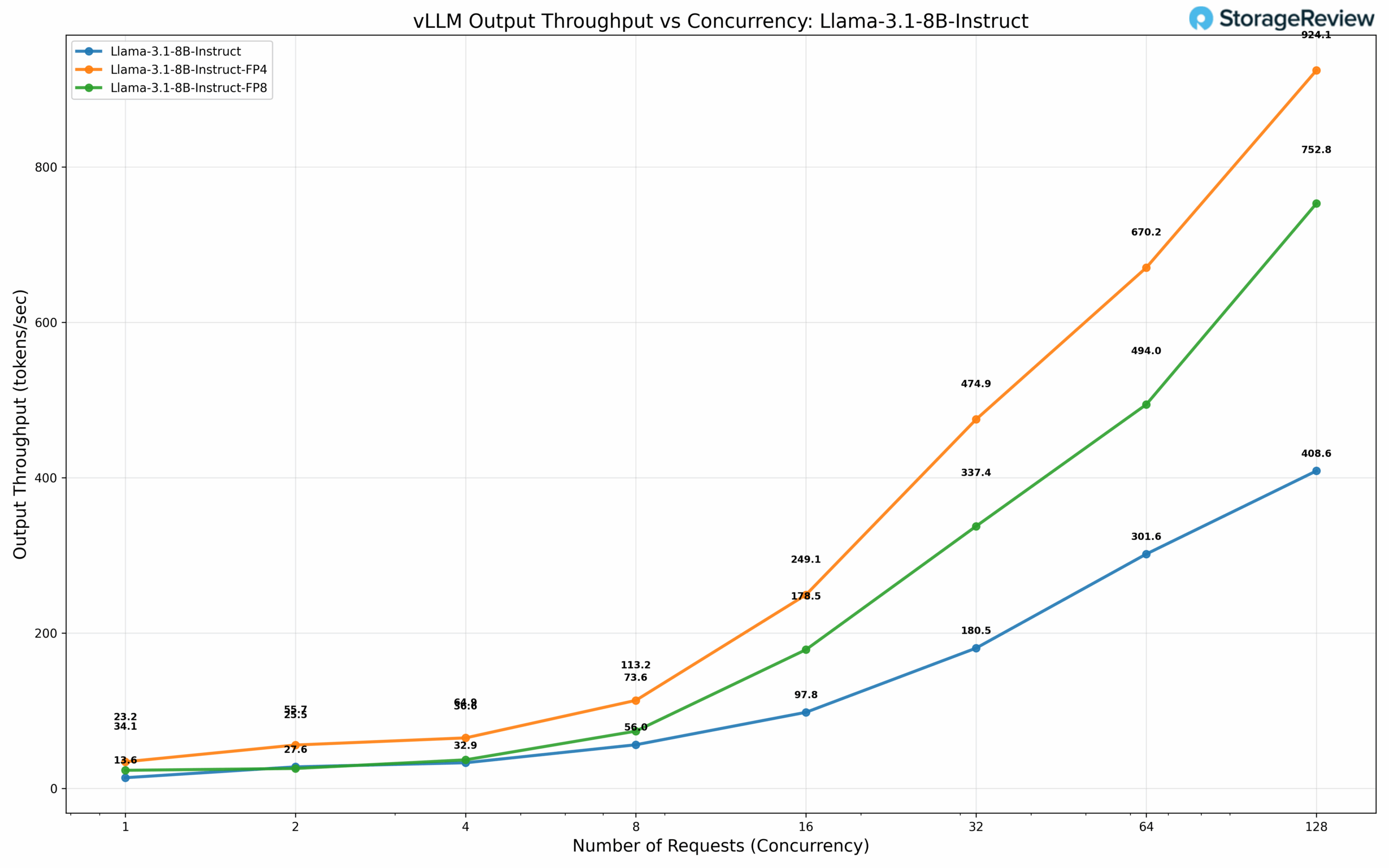
The Llama 3.1 8B architecture reveals markedly different performance characteristics across quantization strategies. At BF16 precision, the model delivers 13.6 tok/s at concurrency 1, expanding to 408.6 tok/s at 128 concurrent requests. Transitioning to FP8 quantization yields 23.2 tok/s and 752.8 tok/s at concurrency levels 1 and 128, respectively—representing an 84% throughput improvement at scale. The FP4 configuration pushes performance further, achieving 34.1 tok/s and 924.1 tok/s at the same concurrency levels, demonstrating that aggressive quantization strategies can deliver 2.3x performance gains over baseline precision while maintaining acceptable model quality for many production workloads.
Microscaling Datatype
Microscaling represents an advanced quantization approach that applies fine-grained scaling factors to small blocks of weights rather than uniform quantization across large parameter groups. NVIDIA’s NVFP4 format implements this technique through a blocked floating-point representation where each microscale block of 8-32 values shares a common exponent as a scaling factor. This granular approach preserves numerical precision while achieving 4-bit representation, maintaining the dynamic range critical for transformer architectures. The format integrates with NVIDIA’s Tensor Core architecture, enabling efficient mixed-precision computation with on-the-fly decompression during matrix operations.
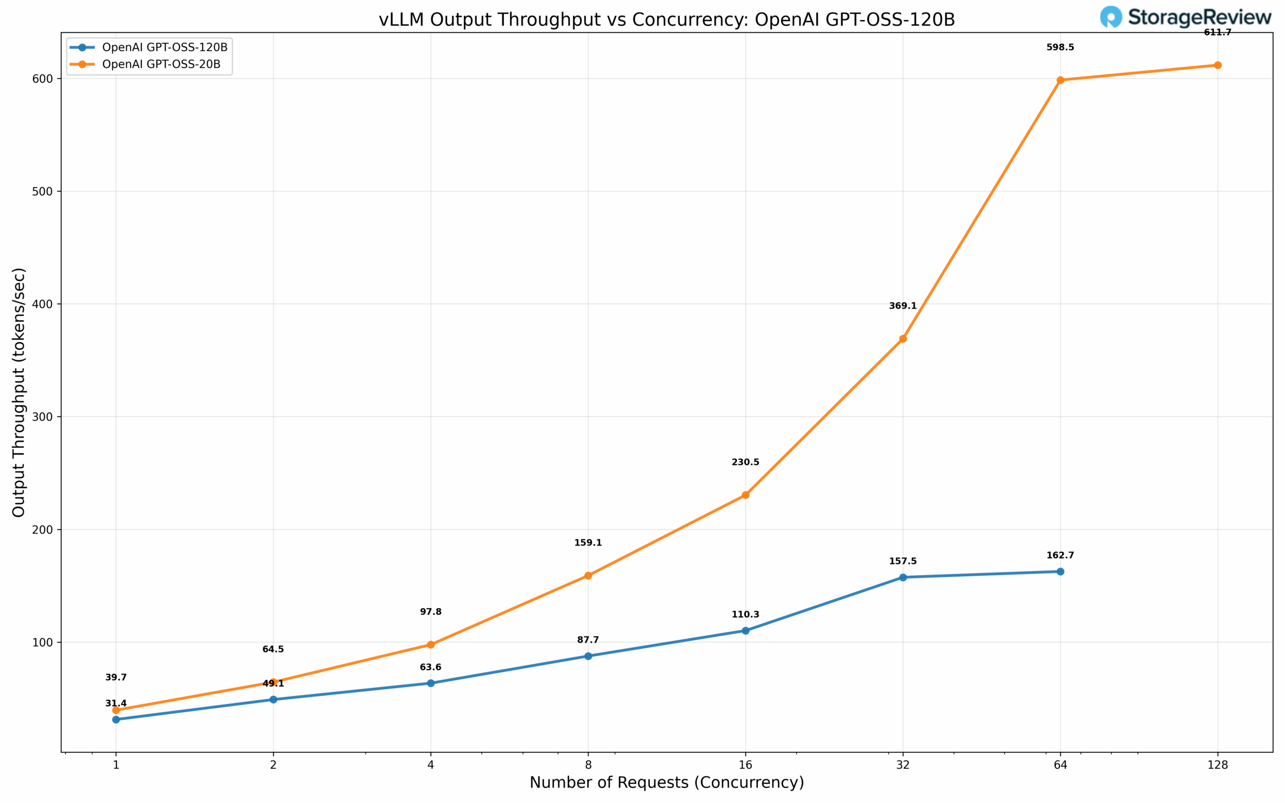
We evaluated OpenAI’s GPT OSS models at 20B and 120B parameter scales using NVFP4 quantization. The 20B parameter model achieves 39.7 tok/s at concurrency 1, scaling to 611.7 tok/s at 128 concurrent requests. The 120B parameter variant delivers 31.4 tok/s at concurrency 1 and 162.7 tok/s at 64 concurrent requests.
Note: The output throughput is the throughput across requests and not per request throughput.
Due to limited time we were not able to finish our TensorRT tests, keep an eye out for follow up pieces with the spark where we will explore performance on more inference frameworks.
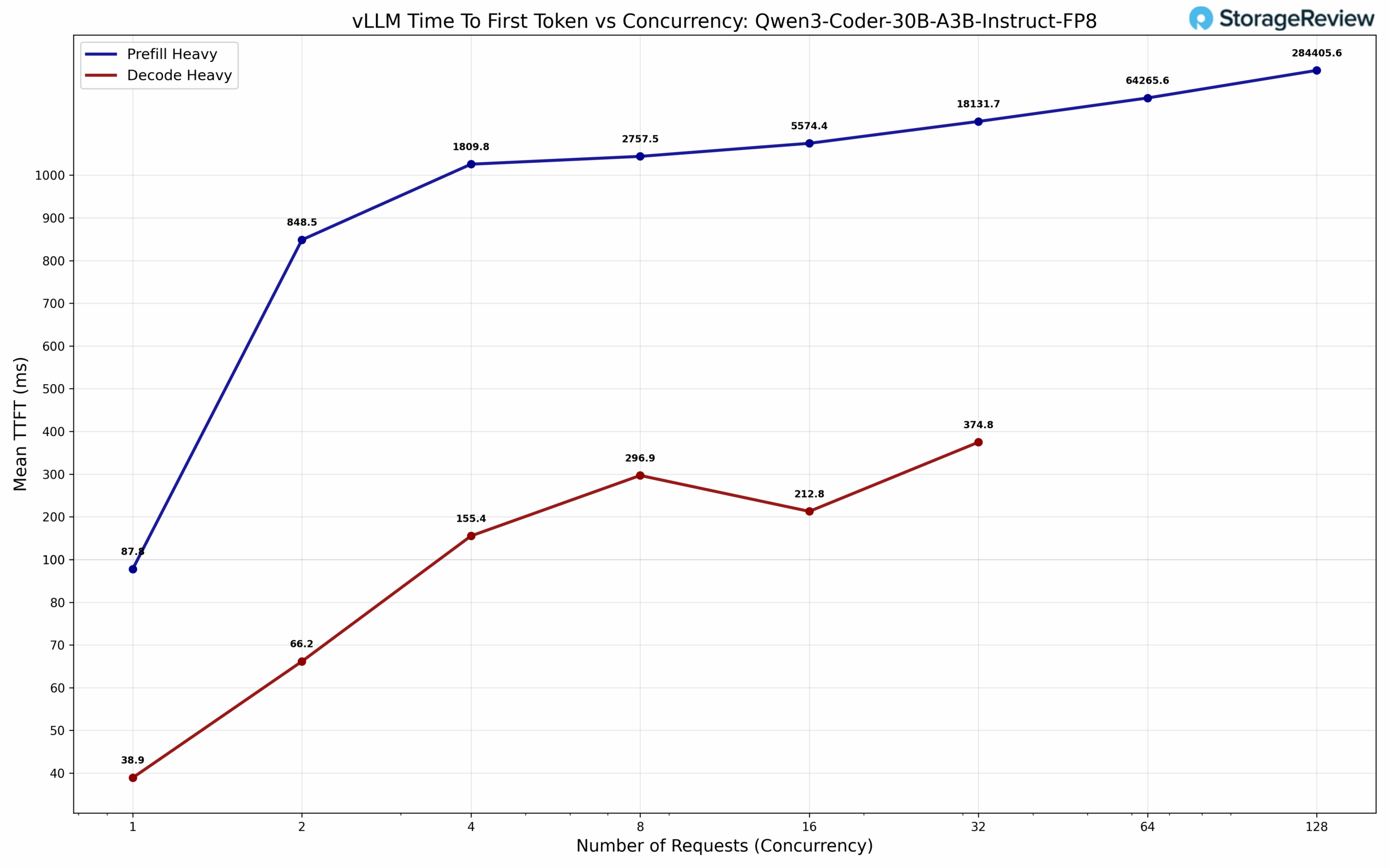
Prefill and Decode Heavy Inference
LLM inference can be fundamentally decomposed into two distinct computational phases, each exhibiting markedly different performance characteristics and resource utilization patterns. The prefill phase processes the entire input prompt in a single parallel operation, computing attention mechanisms across all input tokens simultaneously a compute-intensive operation that fully saturates tensor cores and computational units. Conversely, the decode phase generates output tokens autoregressively, producing one token at a time through sequential operations that exhibit lower computational intensity but place substantial demands on memory bandwidth as the model must repeatedly access weights and the growing key-value cache. This creates fundamentally different bottleneck profiles: prefill operations are typically compute-bound, while decode operations become memory bandwidth-intensive, making them particularly susceptible to memory subsystem constraints.
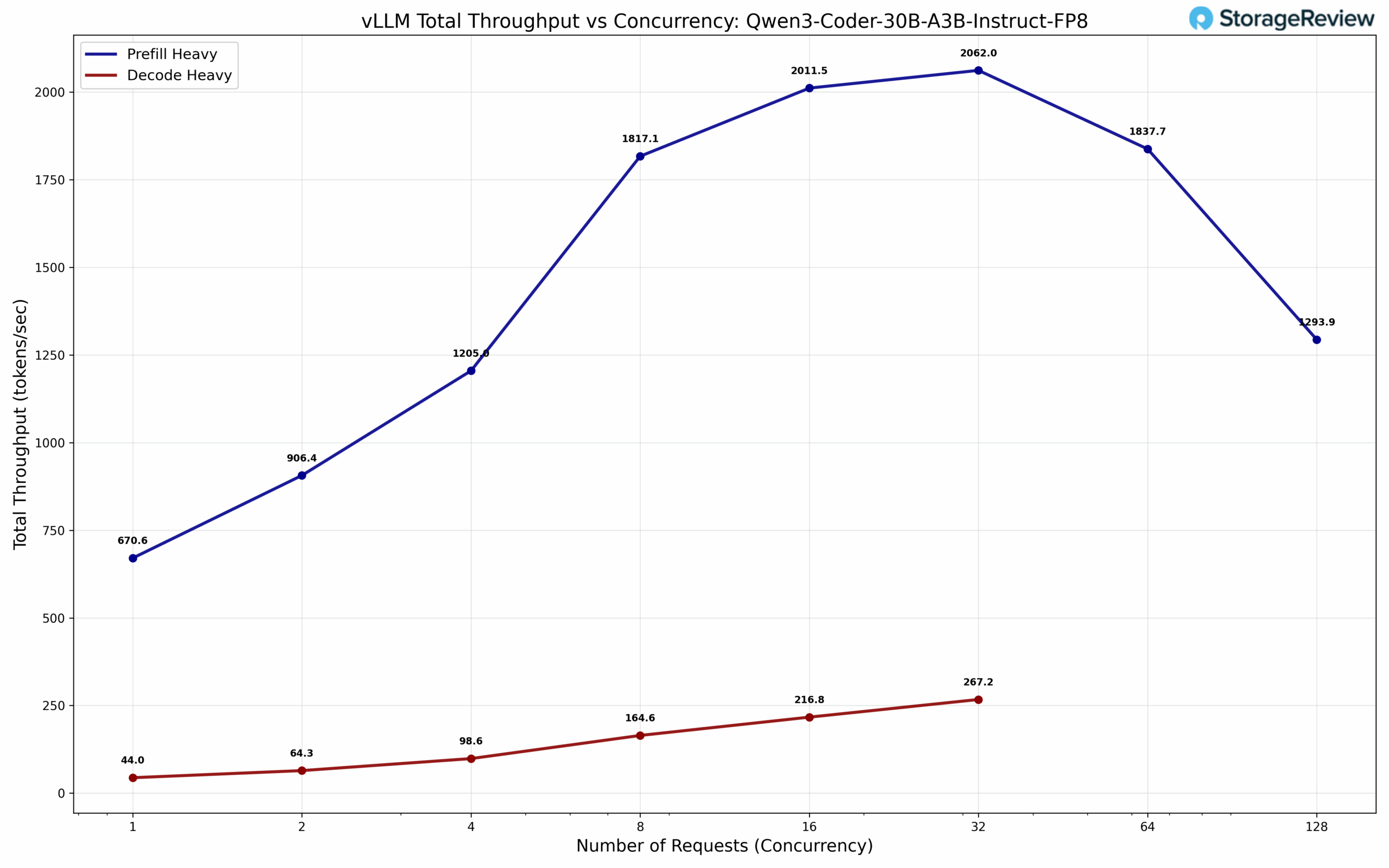
We conducted comprehensive testing across two distinct workload profiles: decode-heavy inference with 512 input tokens and 8,192 output tokens, and prefill-heavy inference with 8,192 input tokens and 512 output tokens. The performance characterization reveals expected architectural trade-offs: the Spark demonstrates competitive throughput on prefill-heavy workloads where compute resources remain the primary bottleneck, but exhibits reduced performance on decode-heavy scenarios. This performance differential aligns precisely with the memory bandwidth constraints. Decode operations’ sequential nature and intensive memory access patterns directly expose the bandwidth limitations inherent in the Spark’s architecture. These results provide critical context for interpreting the MAMF measurements in the next section, as both benchmark suites consistently identify memory bandwidth as the fundamental performance-limiting factor in real-world inference deployments.
Maximum Achievable Matmul FLOPS (MAMF)
MAMF (Maximum Achievable Matmul FLOPS) is a practical performance metric designed to measure the realistic peak floating-point operations per second that can be achieved on machine learning accelerators during matrix multiplication operations, offering a more accurate benchmark than the theoretical peak FLOPS often advertised in hardware specifications. We are using the mamf-finder benchmark by Stas Beckman.
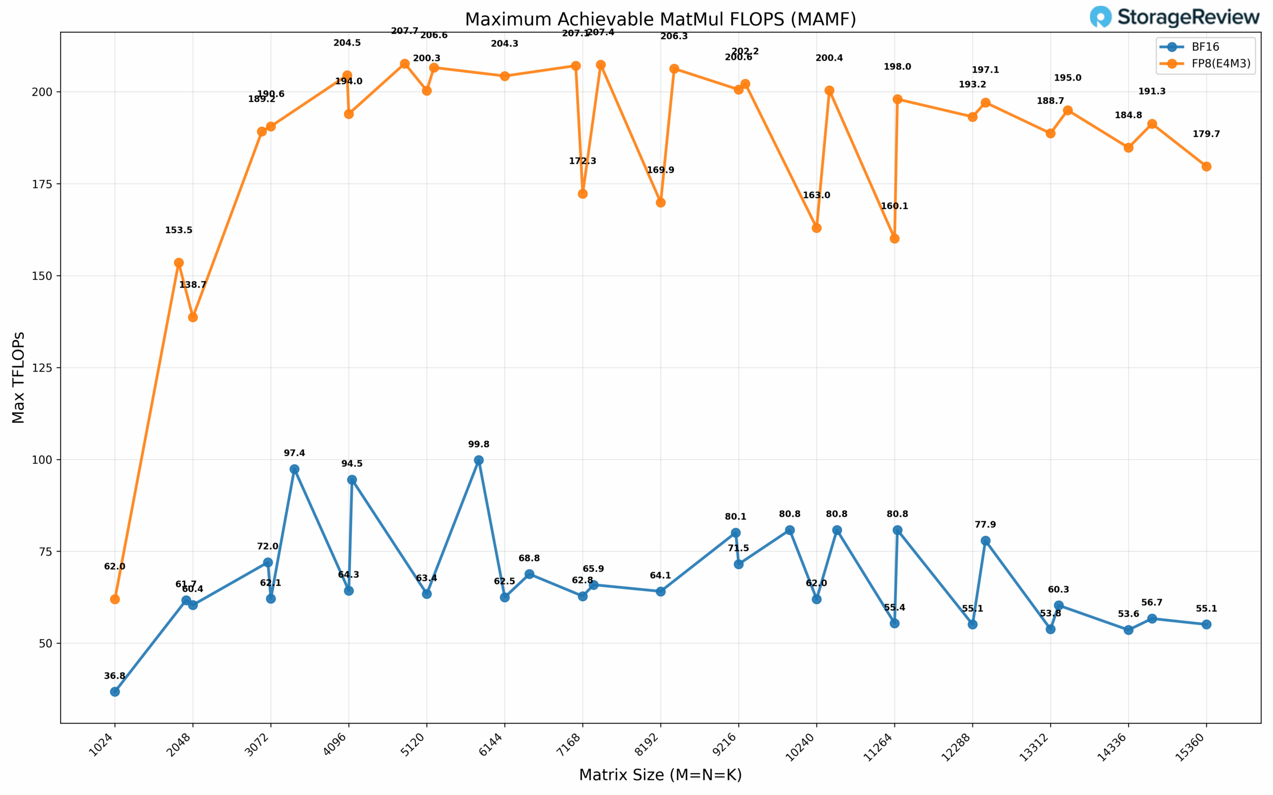
At BF16 precision, we observe a MAMF of 99.8 TFLOPs, while FP8 (E4M3) demonstrates a MAMF of 207.7 TFLOPs. Due to time constraints, we were unable to conduct comprehensive FP4 MAMF characterization; however, extrapolating from observed precision-based scaling patterns, we anticipate an additional 2× performance gain over FP8, yielding approximately 400 TFLOPs for dense FP4 operations. When factoring in 2:1 structured sparsity optimization, this translates to roughly 80% of theoretical FP4 performance capabilities, achieving approximately 800 TFLOPs under sparse computational workloads. It is important to note that these MAMF measurements may fall below theoretically advertised specifications due to many reasons we won’t go into in this review.
GPU Direct Storage
One of the tests we conducted on the Spark was the MagnumIO GPU Direct Storage (GDS) test. GDS is a feature developed by NVIDIA that allows GPUs to bypass the CPU when accessing data stored on NVMe drives or other high-speed storage devices. Instead of routing data through the CPU and system memory, GDS enables direct communication between the GPU and the storage device, significantly reducing latency and improving data throughput.
How GPU Direct Storage Works
Traditionally, when a GPU processes data stored on an NVMe drive, the data must first travel through the CPU and system memory before reaching the GPU. This process introduces bottlenecks, as the CPU becomes a middleman, adding latency and consuming valuable system resources. GPU Direct Storage eliminates this inefficiency by enabling the GPU to access data directly from the storage device via the PCIe bus. This direct path reduces the overhead associated with data movement, allowing faster and more efficient data transfers.
AI workloads, especially those involving deep learning, are highly data-intensive. Training large neural networks requires processing terabytes of data, and any delay in data transfer can lead to underutilized GPUs and longer training times. GPU Direct Storage addresses this challenge by ensuring that data is delivered to the GPU as quickly as possible, minimizing idle time and maximizing computational efficiency.
In addition, GDS is particularly beneficial for workloads that involve streaming large datasets, such as video processing, natural language processing, or real-time inference. By reducing the reliance on the CPU, GDS accelerates data movement and frees up CPU resources for other tasks, further enhancing overall system performance.
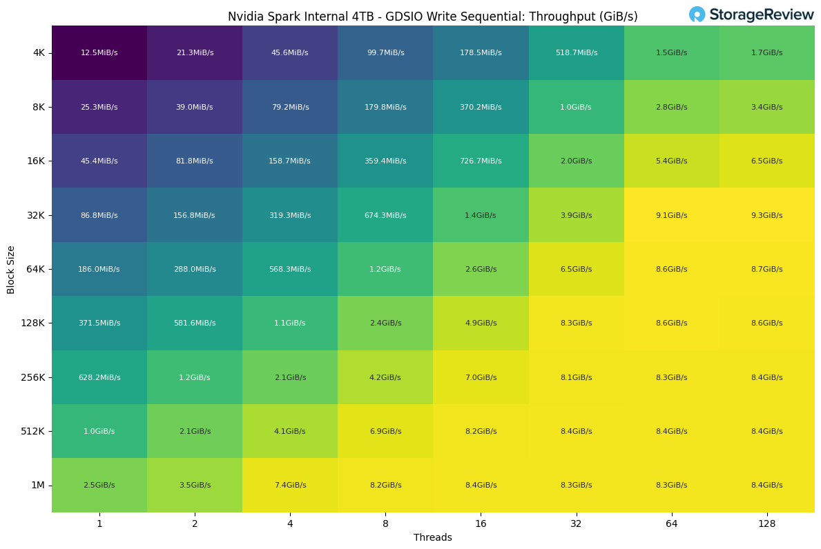
GDSIO – Internal 4 TB M.2
The NVIDIA DGX Spark has an interesting choice for storage. For size considerations inside the small case, NVIDIA went with the less-common Gen5 2242 M.2 SSD. For readers not familiar with this type of SSD, it is a shorter 42mm version compared to 80mm which is more common in the desktop space. There are fewer drive choices, with 4 TB being the top-end capacity in this size. The main issue, though, is performance. Small SSDs, such as the 2242 and 2230 models, prioritize size considerations, with drive speeds taking a secondary role. They are common in portable game consoles, tablets, and some notebooks.
There isn’t a lot of space on the 2230 and 2242 SSD PCB, resulting in less room for controllers, DRAM, and NAND packages. We observed some of these tradeoffs during our testing. When applying our GDSIO workload in a 1 TB or 128 GB footprint, the SSD would lock up and require re-imaging the Spark. Lowering the test footprint to 64 GB, as well as lowering the higher-thread count, got around this issue. These issues generally don’t come up with more common high-performance 80mm SSDs.
Looking into the Sequential Read performance of the internal drive, we see the highest throughput at 1M block size with 16 threads, achieving 11.4 GiB/s.
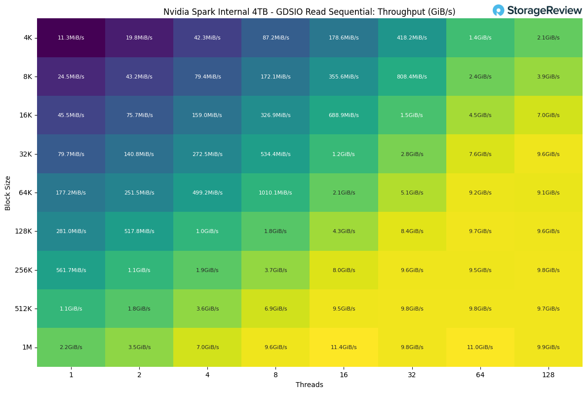
Looking at Sequential Write performance, the drive achieves the highest throughput at 32k block size with 128 threads. At larger block sizes, the performance appears to plateau, averaging around 8.3 GiB/s.
For buyers looking to purchase the NVIDIA DGX Spark for heavier development work, especially businesses that might make small clusters out of them, we’d highly recommend going the route of leveraging the onboard 200Gb NVIDIA ConnectX-7 NIC.
GDSIO – NVMe-oF over RDMA
For NVMe-oF RDMA testing with the NVIDIA DGX Spark, we utilized PEAK:AIO’s software to create an NVMe-oF target on a Dell PowerEdge R770 with six Micron 9550 3.84TB SSDs and connected over RDMA. As we previously mentioned, the Spark’s CX7 NIC has its quirks, and due to time constraints, we were only able to test the Spark with 100G connectivity. Both the Spark and PEAK:AIO can achieve significantly higher numbers. We will conduct additional storage and network testing with the Spark in subsequent pieces.
Looking into the Sequential Read performance of the internal drive, we see the highest throughput at 128k block size with 32 threads, achieving 12.1 GiB/s.
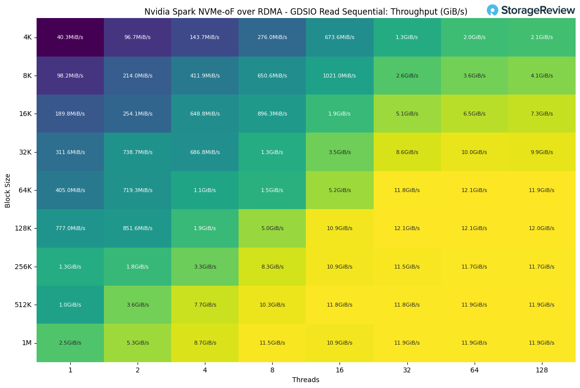
Looking at Sequential Write performance, the drive achieves the highest throughput at 128k block size with 16 threads. At larger block sizes, the performance appears to plateau, averaging around 11.3 GiB/s.
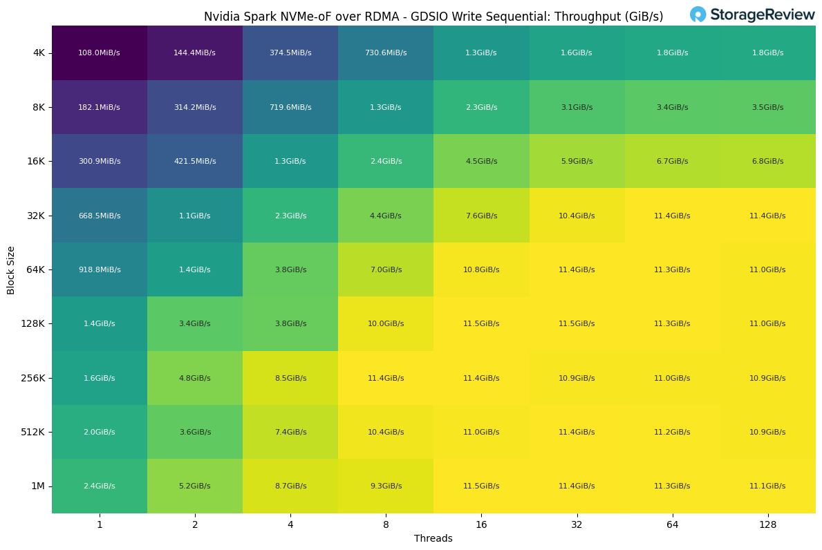
There is a lot of nuance with these results, we are only seeing half of the theoretical maximum due to aforementioned time related and networking related reasons. Additionally highest throughput at 128k blocksize is influenced by multiple factors like the enterprise drives we utilized or how PEAK:AIO handles this IO, your milage may vary and we intend to do more through testing with spark in the future.
Day-One Software Ecosystem
NVIDIA and other vendors have invested substantially in software readiness, a stark departure from typical hardware launches where early adopters navigate incomplete documentation and missing tooling. Spark launches with comprehensive playbooks covering common workflows: ComfyUI for diffusion models, TRT-LLM for optimized inference, Ollama with Open WebUI for local model serving, Unsloth for fine-tuning, and multi-agent architectures with LangGraph.
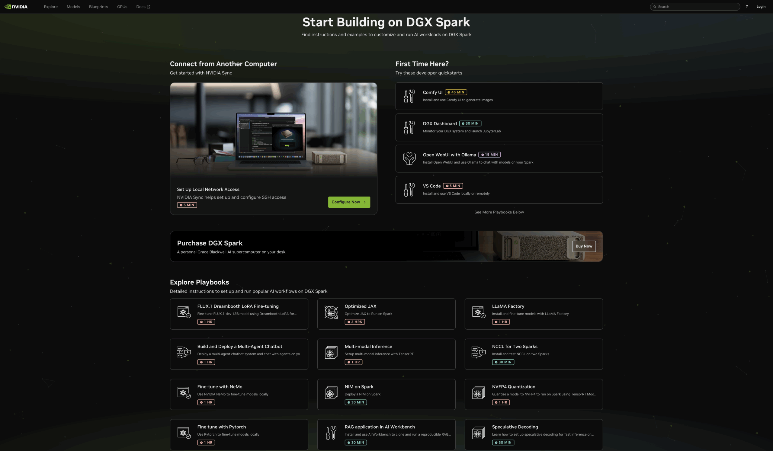
This software maturity transforms the evaluation experience. Rather than spending days configuring environments, developers can immediately assess whether Spark meets their requirements by running representative workloads. The playbooks provide not just instructions but containerized environments, sample datasets, and expected performance metrics.
Availability and OEM systems
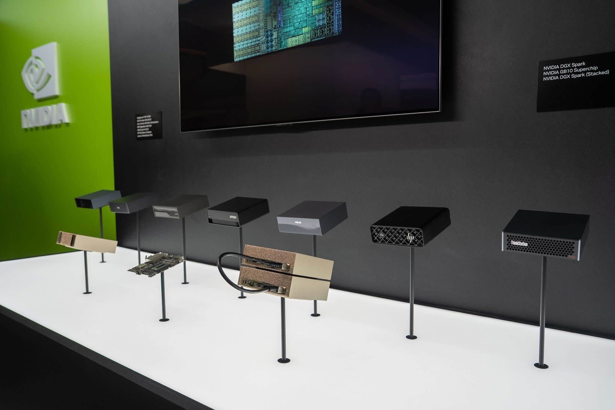
NVIDIA’s Founders Edition is available to order at $3,999 for the 4TB configuration, and general availability begins October 15. Alongside NVIDIA’s own unit, several GB10 desktops are arriving from the big OEMs. The core hardware will be pretty similar across all of the OEMs, but there may be a little wiggle room for them to differentiate, though most of the pricing variance will likely come from storage selection. We’ve already seen many announcements, including the Dell Pro Max with GB 10, Lenovo ThinkStation PGX, Acer Veriton GN100, and ASUS Ascent GX10.
Source: Nvidia
Conclusion
The NVIDIA DGX Spark represents a fundamental inflection point in the accessibility paradigm of advanced AI computing infrastructure. By consolidating the GB10 Grace Blackwell Superchip’s capabilities: 128 GB unified memory, 1 petaFLOP sparse FP4 performance, fourth-generation RT Cores, and ConnectX-7 networking into a 240W, 1.13-liter appliance priced at $3,999, NVIDIA has effectively collapsed the barriers that historically segregated datacenter-class AI capabilities from individual researchers and small development teams.
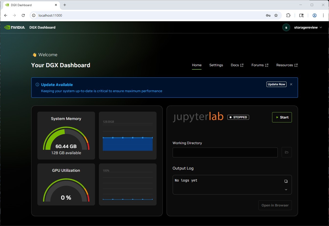
The validated appliance approach addresses a persistent friction point in AI infrastructure deployment: the operational overhead of maintaining custom configurations. Organizations deploying Spark units benefit from NVIDIA’s comprehensive testing and validation of the complete stack, including DGX OS, CUDA toolkit, framework containers, and hardware firmware, thereby eliminating the configuration debt that plagues custom workstation builds. The DGX Dashboard’s integrated update management, system monitoring, and JupyterLab provisioning further reduce operational burden, while NVIDIA Sync’s automatic SSH key distribution and tunnel management make remote access genuinely frictionless. For scaling organizations, this translates to measurably faster onboarding: new researchers receive standardized hardware, connect to existing infrastructure via the validated two-node clustering configuration, and begin productive work within hours rather than days of troubleshooting driver conflicts or network fabric configuration.
DGX Spark already delivers real AI horsepower in a compact, quiet appliance, and our early results show why it matters for teams that want serious capability without datacenter overhead. The story is just getting started. We plan to expand our testing with the 200G fabric, NVMe-oF targets, and multi-node clustering to explore scaling efficiency, larger model footprints, and shared storage architectures. As the software and partner ecosystem matures, we expect Spark deployments to evolve from powerful single-node setups into tightly integrated, high-throughput mini clusters that further enhance this platform.


 Amazon