

There are two stories in the Dell Pro Max 16 Plus, and they pull in opposite directions. One is a top-tier mobile workstation: Intel’s 24-core Core Ultra 9 285HX, up to 256GB of CAMM2 memory, three M.2 slots, NVIDIA RTX PRO Blackwell graphics up to the 5000-series with 24GB of GDDR7, MIL-STD-810H build, and a chassis that Dell has clearly poured engineering into.
The other is the SKU under review, which trades the GPU for a Qualcomm AIC100 PC Inference Card, a dual-SoC module built around 2019-era Cloud AI 100 silicon, and a software stack that turns most modern inference workloads into a painful exploration. This is a cautionary tale about what happens when a flagship chassis gets paired with the wrong accelerator, and why customers need to understand the software stack behind an AI solution before they sign the purchase order. Before we get to why, let’s look at the laptop as a whole.
The Pro Max 16 Plus sits at the top of Dell’s Pro Max workstation lineup, delivering more raw power than both the entry-level Pro Max 16 and the slimmer Pro Max 16 Premium. At its core is Intel’s scalable Core Ultra 9 285HX, a 55-watt, 24-core chip with a 5.5GHz turbo boost. All CPU configurations support Intel vPro Enterprise, reinforcing the laptop’s enterprise-grade credentials. Pricing starts at $2,779.
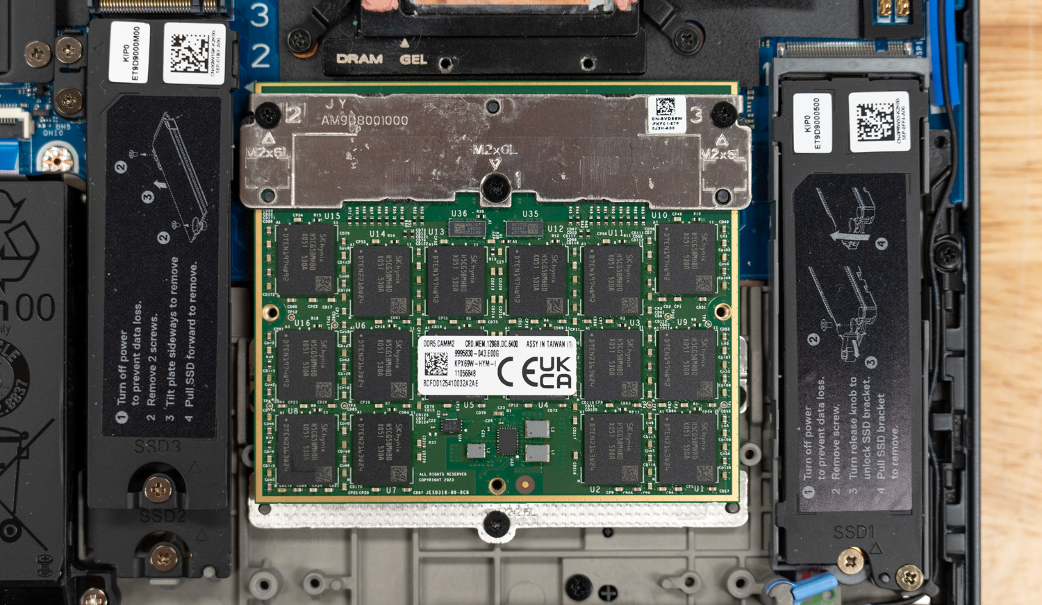
Graphics options span integrated Intel graphics through NVIDIA’s Blackwell-based RTX PRO 1000, scaling all the way up to the RTX PRO 5000 we reviewed previously, which features an impressive 24GB of GDDR7 memory. Storage and memory configurations are equally generous: up to 12TB across three M.2 Gen5 slots, and up to 128GB of DDR5-6400 memory delivered via Dell’s CAMM2 module.
Display choices range from a basic 1920 x 1200 IPS panel to the vivid 3840 x 2400 OLED touchscreen. A mid-tier 1920 x 1200 option sits between the two, adding 500 nits of brightness, a 120Hz variable refresh rate, and full DCI-P3 coverage. With over 100 ISV certifications, creative professionals can expect their applications to run smoothly.
Security features are enterprise-ready, including a fingerprint reader, Smart Card support, NFC, an 8MP IR camera for facial recognition, and Dell’s Control Vault 3. A standard three-year warranty rounds out the package, underscoring the laptop’s role as a serious tool for serious work.
Dell Pro Max 16 Plus Specifications
| Specification | Dell Pro Max 16 Plus |
|---|---|
| Platform | |
| Processor | Intel Core Ultra 5 245HX Intel Core Ultra 7 265HX Intel Core Ultra 9 285HX |
| Operating System | Windows 11 Pro Ubuntu Linux 24.04 LTS |
| Memory | 16GB-128GB CSoDIMM or CAMM2, 1 slot |
| Graphics and AI Acceleration | |
| Graphics Card | Intel Integrated Graphics NVIDIA RTX PRO 1000 8GB NVIDIA RTX PRO 2000 8GB NVIDIA RTX PRO 3000 12GB NVIDIA RTX PRO 4000 16GB NVIDIA RTX PRO 5000 24GB Qualcomm AI Cloud 100 64GB (2x 32GB) |
| Storage and Display | |
| Storage | Up to 3x M.2 SSD, 4TB each Available RAID 0/1/5 |
| Display | 16-inch 16:10 1920×1200, 300-nit, 45% NTSC, 60Hz, non-touch 1920×1200, 500-nit, 100% DCI-P3, 120Hz VRR, non-touch 3840×2400, 500-nit, OLED, touch |
| Connectivity and Power | |
| Camera | 8MP IR |
| Wireless Networking | Intel Wi-Fi 7 BE200, with or without Bluetooth 5.4 Available mobile broadband |
| Battery | 6-cell 96Whr |
| Power Adapter | 165W or 280W |
| Security and Physical | |
| Security Features | IR webcam Fingerprint reader Smart Card reader NFC Control Vault 3 |
| Dimensions and Weight | 1.22 by 10.18 by 14.17 inches Starting weight: 5.63 pounds |
| Warranty | Standard three years, next business day onsite repair |
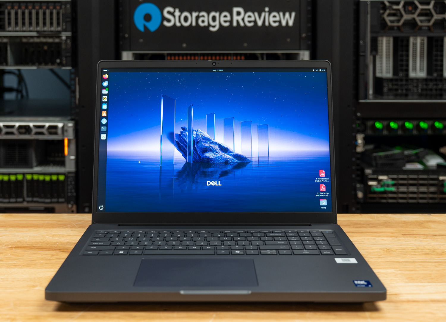
Build and Design
Like the previous unit we reviewed, the Pro Max 16 Plus is unapologetically rugged, holding a MIL-STD-810H certification for durability in demanding environments. Dell’s material mix leans heavily into sustainability, incorporating post-consumer recycled plastic, recycled magnesium and cobalt, and bio-based plastics. In hand, the chassis feels exceptionally rigid, with no detectable flex. In short, it’s built like a tank.
This is a substantial machine. At 1.22 inches thick (including its feet) and starting at 5.63 pounds, it isn’t built for frequent travel, though its 10.18 x 14.17-inch footprint is reasonably compact for a 16-inch, 16:10 display. The webcam sits at the top of the lid, complete with a sliding privacy shutter; our review unit ships with the IR version for facial recognition.
Aesthetically, Dell’s design language is understated to a fault. The gray-black exterior and subtle branding emphasize that this is a product of function over form. The Pro Max Premium line offers more visual flair at the cost of performance and expansion.
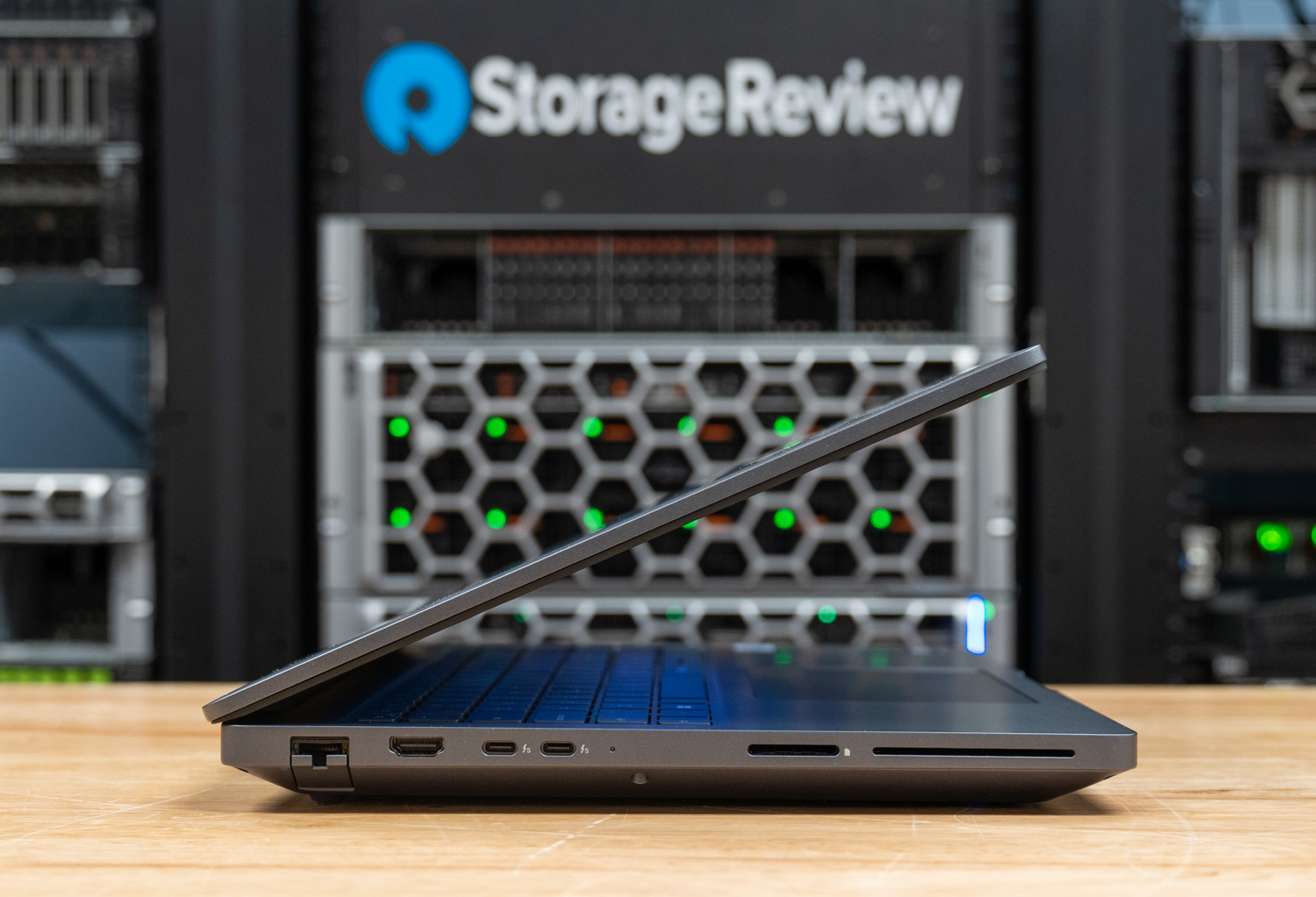
The comprehensive port selection starts on the left edge:
- 2.5Gbps RJ45 Ethernet
- HDMI 2.1 output
- Two Thunderbolt 5 (USB-C) ports
- SD card reader
- Optional SmartCard slot
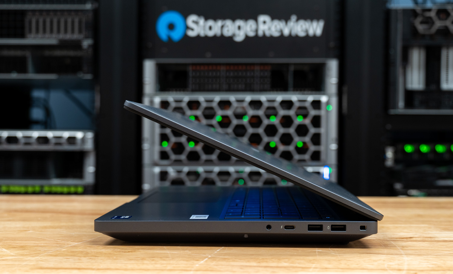
On the right:
- 3.5mm audio jack
- Thunderbolt 4 (USB-C)
- Two USB 3.2 Gen1 Type-A ports
- Lock slot
There are no ports on the rear edge. Wireless connectivity is handled by Intel’s BE200 module, supporting Wi-Fi 7 and Bluetooth 5.4. Bluetooth can be omitted in custom configurations, and 5G mobile broadband is also available.
Screen and Input Devices
Our review unit features Dell’s 16-inch 1920×1200 display with a 120Hz VRR panel that looks excellent in daily use. Colors are vibrant, and with 100% DCI-P3 coverage, it’s well-suited for color-sensitive workflows once calibrated. The 500-nit brightness also helps the display remain comfortable to use in brighter office or studio environments.
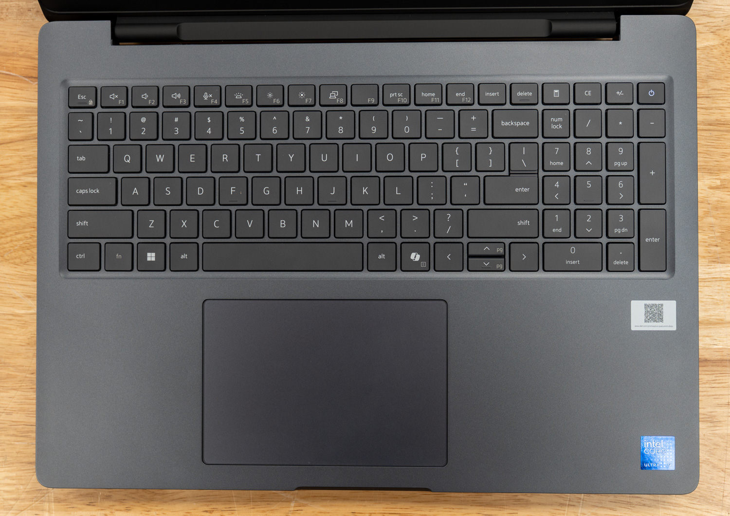
Dell’s keyboard is well-suited for long typing sessions, with full-size keys that deliver a light, responsive feel and crisp tactile feedback. White backlighting keeps it visible in dim environments. The layout is largely conventional, but the uneven sizing of the arrow keys can cause occasional mispresses, and the placement of the Home and End keys is a particular drawback; they share space with F11 and F12, so enabling Fn-Lock (Fn + Esc) to prioritize the function row forces a Fn + F11 or F12 press to access them. Dedicated Page Up and Page Down keys would have been welcome; instead, they’re secondary functions of the up and down arrows, which are already the most awkward keys in the cluster. The power button, located at the top right, doubles as a fingerprint sensor.
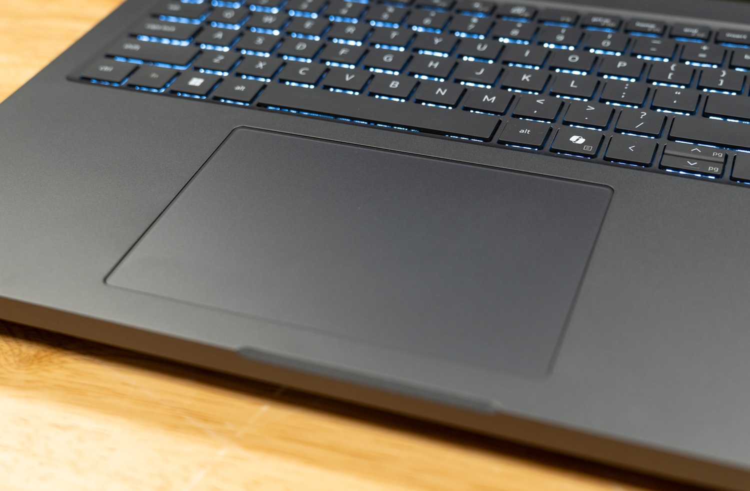
The generously sized touchpad complements the 16-inch form factor. Its smooth anti-glare surface tracks accurately, and palm rejection performed flawlessly throughout testing.
Upgradeability
The Pro Max 16 Plus is built with expansion in mind, offering substantial upgrade potential. It features three M.2 Gen5 slots for storage, a CAMM2 slot for memory upgrades, and several modular components, including replaceable USB-C ports.
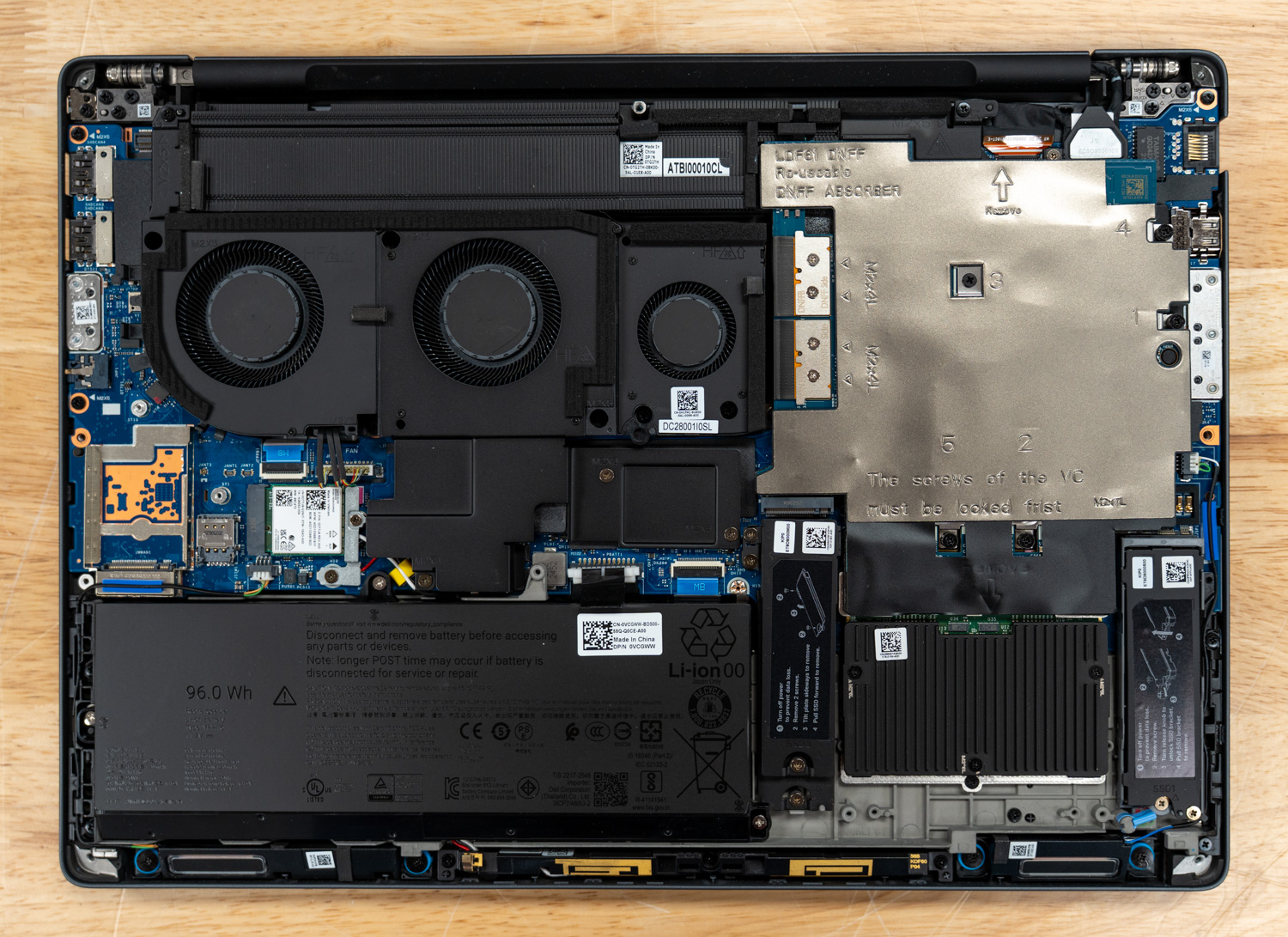
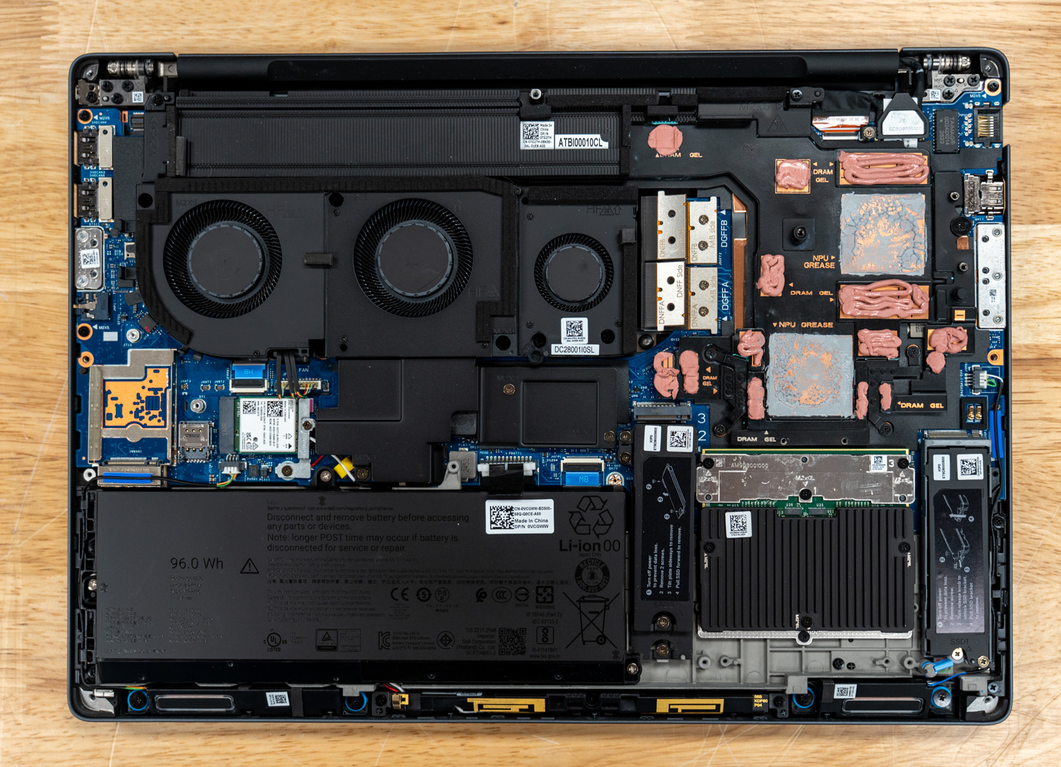
Accessing the internals is straightforward: remove the perimeter screws and lift the bottom panel from back to front. Inside, you’re greeted by a robust three-fan cooling system and a sizable 96Whr battery. The CAMM2 memory module sits at the bottom right, positioned beneath a dedicated heatsink and flanked by the M.2 slots. It’s difficult to tell from the photo, but the M.2 slot on the left is actually a stacked slot that houses two drives in the same footprint. The M.2 wireless card, also user-replaceable, sits just above the battery.
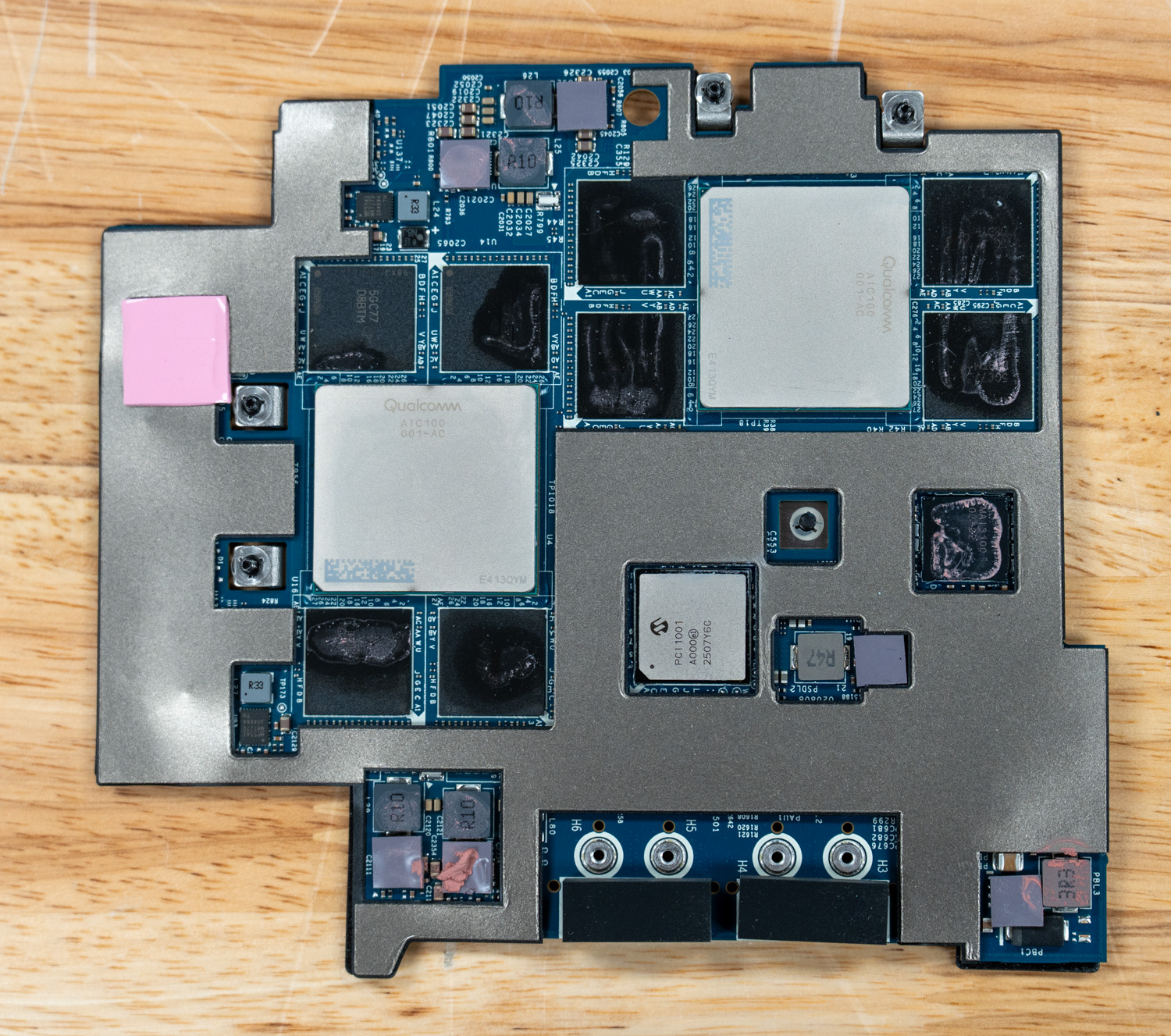
The Star of the Show: Qualcomm AIC100
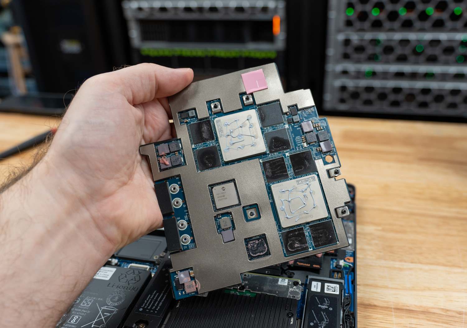
The Dell SKU under review ships with the Qualcomm AI 100 NPU, a single module that houses two Qualcomm Cloud AI 100 SoCs side by side. Each SoC contributes 16 AI cores for a combined 32 across the module, and each carries its own 32GB of LPDDR4x, presented to the host as two individual NPUs.
Dell and Qualcomm advertise roughly 450 TOPS of INT8 throughput and the ability to run models in the 100-billion-parameter range, with Dell publicly demonstrating Llama 4 Scout (109B parameters, MoE) running locally on the laptop. The two SoCs communicate with the host through the Linux QAIC accelerator driver, with firmware blobs upstreamed into linux-firmware.
So far, so reasonable. The numbers, in isolation, are big. The problem is the silicon underneath those numbers.
Qualcomm announced the Cloud AI 100 in April 2019, sampled it in late 2020, and began shipping it commercially in the first half of 2021. The chip is built on a 7nm node and uses four 64-bit LPDDR4X controllers running at 2100 MHz (LPDDR4X-4200), delivering 136 GB/s of memory bandwidth per SoC, per Qualcomm’s own Cloud AI architecture documentation.
It was originally designed with the PCIe form factor in mind. Stuffing two of these chips onto a custom module and dropping it into a 2025 laptop does not change the underlying trade-offs. This is 2019-era silicon with 2019-era memory technology, refreshed and renamed but architecturally the same family. By the time it landed in the Dell Pro Max 16 Plus, the rest of the industry had moved through HBM2e, HBM3, HBM3e, and LPDDR5X, and is now heading toward GDDR7 and HBM4 on serious AI accelerators.
But the deeper issue matters more than memory bandwidth. There are many brilliant chip designs and engineering teams in the industry that understand the AI inference problem at a very deep level, and the Cloud AI 100 architecture itself may well be competent. The trouble is that the software engineers who actually make a product live or die have already invested heavily in another ecosystem: CUDA. Unless there is a strong incentive to switch, developers stick with the toolchain that already has great support, documentation, and community help. NVIDIA captured the developer base early and built an enormous community around it. AMD spent years lagging on this front, but the recent ROCm revs are genuinely excellent, and the gap is closing. Solutions like Modular’s Mojo and MAX even let you target NVIDIA or AMD with the same code, and sometimes beat the native runtimes. Every other accelerator, though, struggles with public adoption due to a lack of software backing.
Public adoption is the operative phrase. Large organizations like Google can pour billions into XLA and JAX to make TPUs sing. Well-funded private startups and AI labs can write custom kernels for their own narrow set of models and not care that nobody else can replicate the stack they aren’t building for infinite public use cases; they’re building for the problems they face. For a public consumer, or even most enterprises, an accelerator without a thriving public developer ecosystem is functionally useless. You will burn weeks trying to get your model onto it, and the moment Hugging Face ships a new architecture, you will be staring at a recompile job (or an unsupported-model error) while everyone on CUDA and ROCm has day-zero support.
So let me say it plainly: the AIC100 in this laptop is dead in the water. No individual should buy it. No organization should buy it unless it has the engineering resources and the explicit intent to spin up inference from scratch for its specific workload, and has accepted that it is signing up to maintain that stack itself.
The Software and Tooling Reality
To understand why that recommendation is as harsh as it is, you have to look at what shipping inference on this card actually involves.
The user-facing pieces are split into two SDKs and one wrapper library. The Qualcomm Cloud AI Platform SDK ships the kernel driver (the upstream accel/qaic driver in mainline Linux), the device firmware, the on-card runtime, and low-level APIs. The Apps SDK sits on top and provides the qaic-exec compiler, the qaic-runner inference CLI, ONNX Runtime integration via a QAIC execution provider, Python bindings, and a fork of vLLM. The Qualcomm efficient-transformers library, also called QEfficient, is a Hugging Face Transformers wrapper that reimplements popular LLM architectures with the static shapes, KV cache layouts, and graph transformations required by the AIC100. Qualcomm AI Hub is a separate model catalog and compile-as-a-service product aimed more at Snapdragon-class devices than the AIC100, though it shares branding.
The compile path is rigid. You take a PyTorch model, export it using torch.export or ONNX, and feed it to qaic-exec with flags such as -convert-to-fp16, -mxfp6-matmul, a batch size, a context length, and a target SoC count. The compiler does ahead-of-time scheduling and memory placement, then emits a QPC, a Qualcomm Program Container, a sealed binary that pins memory layout, KV cache shape, batch size, prefill sequence length, and context length. There is no JIT. Per Qualcomm’s own LLM documentation, the ahead-of-time AI 100 compiler pre-allocates device resources based on prompt length, generation length, KV cache, and batch size, and the Cloud AI 100 supports only static input shapes. Any change to those compile-time parameters triggers another full compile, which can take many minutes for small models and hours for large ones.
The list of supported architectures is very short. The QEfficient library and the Zentree-hosted prebuilt QPC catalog that Dell points customers to largely cover older models, and only a handful are worth using in 2026.
Newer FP8-native checkpoints require requantization. If a model ships natively in MXFP4, as the popular GPT-OSS models do, you are looking at a conversion-and-recompile pipeline rather than dropping the weights in. None of this is impossible to work around if you are willing to do the work, but it is a constant tax.
Then there is the concurrency problem, which is where the laptop falls apart, even for developers focused on out-of-the-box performance. The Dell-provided container images, which Dell instructs users to pull and run with vLLM, are based on QPCs that Zentree pre-compiled with specific shapes, and the shipped containers only run at concurrency 1. Regardless of input or output sequence shape, you get a single fixed throughput for a given model. Multiple parallel requests do not run concurrently; they are queued and processed in sequence by vLLM. You cannot dynamically batch. You cannot use continuous batching the way vLLM or SGLang gives you for free on Team Red or Green GPUs. To get any concurrency above 1, you have to recompile the QPC with a larger batch size.
Dell’s examples pitch this laptop to developers, and the most popular AI use case for developers today is vibe coding with tools like Claude Code, OpenCode, and the like. A single request to these tools can fan out into multiple parallel LLM calls; out of the box, these NPUs will queue those requests and process them sequentially rather than in parallel, so something that might take seconds on an NVIDIA Spark will take minutes on this setup.
Performance
The system Dell provided for testing has the following configuration:
- Intel Core Ultra 9 285HX CPU
- Qualcomm AIC100 PC Inference Card
- 128GB 6400MTs CAMM2 DDR5
- 4TB SSD
Before any numbers, a methodology note. As described above, the AIC100 runs ahead-of-time-compiled QPCs with a frozen batch size, sequence length, and KV-cache layout. Dell ships this laptop with a curated set of pre-compiled QPCs hosted on Zentree and a vLLM container image that pulls them down on first launch. That set of pre-cooked QPCs, served through Dell’s reference container at concurrency 1, is what an end user actually receives when they unbox the machine and follow Dell’s documentation, and that is the configuration we benchmarked.
We have the tooling to do otherwise. We could pull qaic-exec, take a checkpoint, run it through torch.export, requantize, recompile a QPC with a larger batch size, and feed it back through vLLM. We could write custom kernels against the QAIC accelerator driver if we wanted to. We chose not to, since the overwhelming majority of buyers in this laptop’s target market, developers, AI-curious engineers, and enterprise pilot teams, will not do that work. They will pull the container, run it, and judge the product on what comes out. So that is what we measured.
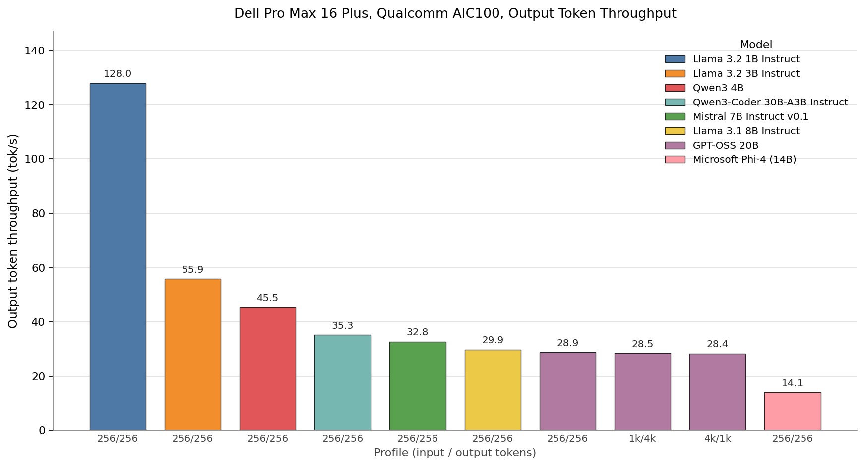
Every bar represents a Qualcomm-compiled QPC running with MXFP6 weights and an MXINT8 KV cache, the precision Dell’s shipped artifacts use across the board. Llama 3.2 1B is the only model on the chart that exceeds 100 TPS, reaching 128 TPS. Llama 3.2 3B follows at 56 TPS, Qwen3 4B at 45 TPS, Qwen3-Coder 30B-A3B at 35 TPS, Mistral 7B at 33 TPS, and Llama 3.1 8B at 30 TPS. GPT-OSS 20B sits at 28.9, 28.5, and 28.4 TPS across the 256/256, 1k/4k, and 4k/1k profiles, confirming what Qualcomm’s documentation promises about the AOT compiler: once a QPC is built for a shape, the decode rate is fixed and prompt length does not move the per-token cost. Phi-4 closes out the chart at 14 TPS.
Although larger models than the ones above will fit on this card, we did not benchmark them. Doing so, for example, with the Llama 4 Scout model, Dell demos publicly, requires dropping precision further to INT4, and in practice, a less-quantized, smaller model will outperform a heavily quantized, larger one across many workloads.
The shipped vLLM container also runs every QPC at batch_size=1, and we confirmed in practice that issuing two simultaneous requests does not double throughput. The second request simply waits in the software queue until the first finishes. There is no continuous batching, in-flight batching, or speculative decoding available in the shipped stack. For coding agents like Claude Code or OpenCode that fan out multiple parallel LLM calls from a single user turn, this single-stream cap turns what should be a few seconds of response time into a multi-minute wall-clock wait. Raising the batch dimension requires recompiling the QPC on the host, which puts us back at the trapdoor we already declined to step through.
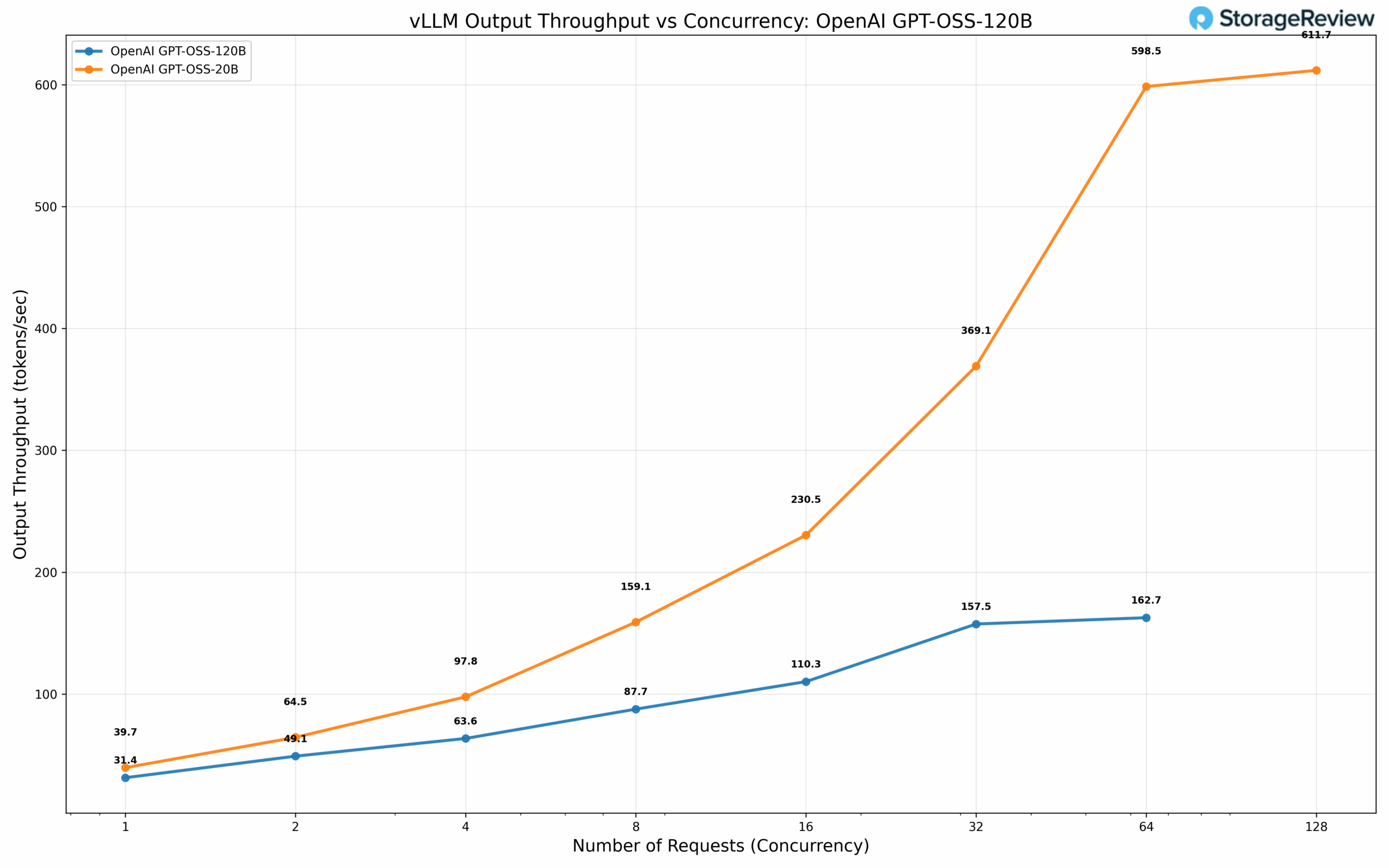
Let’s compare this to the NVIDIA Spark. With 256/256 Input and Output Sequence Length, the Spark can run the 120B model faster than Dell’s Qualcomm AIC 100 can run the 20B model. And this is not even the best numbers the Spark can offer, since these results were collected using the Marlin Kernel on launch software revisions.
The takeaway is narrow. For a single user, a single conversation, and a model small enough that 136 GB/s of LPDDR4X per SoC is not the binding constraint (Llama 3.2 1B and, arguably, Llama 3.2 3B), the AIC100 in this laptop is usable. For anything larger, in the configuration the customer actually receives, the combination of single-stream decode and a static-shape compile pipeline that punishes any shape Qualcomm did not pre-bake leaves this accelerator behind the integrated NPU and integrated GPU on the same Intel Core Ultra HX it sits next to, let alone the discrete NVIDIA SKUs the same chassis can be ordered with.
If we just compare the raw specs for a second, the NVIDIA Spark offers 273GB/s, and we tested the maximum achievable floating-point flops (MAMF) at FP8 (E4M3) at 200TFLOPs on a single chip. The QAIC is advertised to offer 272GB/s across 2 chips and 435 TFLOPS of INT8. So, in theory, these should perform similarly, but the Qualcomm one lags behind due to the software.
Who is this for, and should you buy it
For anyone trying to do serious AI work today, the answer is no. Do not buy this configuration.
Dell’s US store lists the AIC100 SKUs of the Pro Max 16 Plus at $14,871.56 for the top configuration (Core Ultra 9 285HX, 128GB RAM, 4TB SSD), $9,661.56 for a mid configuration (Core Ultra 7 265HX, 64GB, 1TB), and $8,831.56 for the entry AIC100 SKU. All ship Ubuntu Linux only, Windows support coming soon. As tested, the machine lands in the $14,000-$15,000 range.
For reference, NVIDIA’s DGX Spark currently sells for $4,699. For that money, you get a GB10 Grace Blackwell Superchip, 128GB of unified LPDDR5X memory, a 4TB NVMe, a Blackwell GPU, and roughly 1 petaflop of FP4 AI compute, all backed by the full CUDA software stack, TensorRT-LLM, NIM, and the entire NVIDIA ecosystem. A single DGX Spark will outperform the AIC100 in this laptop for almost every realistic AI workload, and it will do so with software that any AI engineer hired this year already knows how to use. For the price of our review unit, you could buy three DGX Sparks, kit each one out with a monitor, peripherals, and a desk, and still have money left over. If small AI isn’t your jam, a Dell Pro Max Tower T2 workstation with Intel 285K, 128GB of DDR5 RAM, and an NVIDIA RTX Pro 6000 GPU is also right around $15,000, depending on the SSD size you pair with it.
It is hard to escape the feeling that Dell has put what amounts to e-waste into an otherwise excellent chassis. The Pro Max 16 Plus with an RTX PRO 5000 is a fantastic mobile workstation. The same machine, with an AIC100, is a messy science experiment under a Dell warranty.
Conclusion
If you are a tinkerer reading this a few years from now and you have stumbled across one of these laptops on a clearance shelf for two or three hundred dollars, by all means, pick it up. The system is repairable and upgradable, the keyboard is good, and getting the AIC100 modules to do something interesting as a weekend project is exactly the kind of low-stakes fun this hardware deserves.
If you are anyone trying to do serious AI work today, configure your Pro Max 16 Plus with literally any other accelerator. An NVIDIA RTX PRO mobile GPU, even the entry-level RTX PRO 1000, will serve you better than the AIC100 modules. The Intel Core Ultra HX’s integrated NPU will serve you better in many practical scenarios because it at least plugs into Windows ML, OpenVINO, and the existing PC AI stack.
One suggestion worth offering to Dell: the Pro Max 16 Plus is an excellent chassis, and the Pro Max line is one of the strongest mobile workstation platforms on the market. The AIC100 SKU, as shipped, does not meet that standard by any stretch. An experimental or developer-preview product line, clearly labeled as such, would give Dell a way to ship novel accelerators to customers who want to play with them, without putting the broader Pro Max name behind a stack that is not ready. The Pro Max brand is worth protecting, and there is a clean way to do that while still finding a home for experimental hardware.


 Amazon