

Two of the three big memory makers are putting money into U.S. semiconductor infrastructure at opposite ends of the production chain. Micron committed up to $3 billion to domestic supply-chain investments in July, anchored by a raw silicon wafer deal in Texas, while SK hynix is preparing to break ground on its advanced HBM packaging plant in Indiana, expected this quarter.
Micron Secures 300mm Raw Silicon Supply with GlobalWafers Partnership
Micron plans to deploy up to $3 billion toward the domestic semiconductor supply chain ecosystem. A central component of this capital allocation includes $500 million in strategic financing directed to GlobalWafers Co., Ltd. This capital will support the development and volume production capabilities of GlobalWafers America’s 300mm raw silicon wafer fabrication facility located in Sherman, Texas.
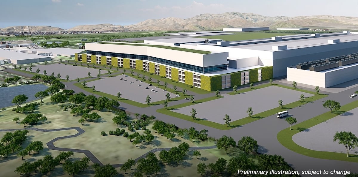
Alongside the financing, Micron and GlobalWafers have finalized a 10-year supply agreement. The multi-year contract ensures dedicated allocation of 300mm raw silicon wafer capacity to support Micron’s long-term memory and storage fabrication roadmaps. The two organizations also plan to evaluate joint development initiatives around next-generation wafer specifications and process innovations to address future manufacturing tolerances.
“Securing a reliable supply of critical input materials is essential to supporting Micron’s long-term growth and technology roadmap,” said Ben Tessone, senior vice president and chief procurement officer at Micron. GlobalWafers chairperson and CEO Doris Hsu framed the domestic angle more sharply, describing the company as currently the only raw silicon wafer supplier in the CHIPS for America Program able to produce advanced 300mm wafers locally. That gives Micron a domestic upstream channel for the substrate its DRAM and NAND output depends on.
SK hynix Preps Its Indiana Advanced Packaging Groundbreaking
At the packaging end of the chain, SK hynix is preparing to break ground on its advanced chip packaging and R&D facility in West Lafayette, Indiana. The ceremony is expected in the third quarter, though SK hynix has not announced a date through its own newsroom. The site sits next to Purdue University on 133.5 acres and is scheduled to begin mass production in the second half of 2028. SK hynix put the investment at $3.87 billion when it signed the agreement with Indiana and now describes it as approximately $4 billion, which the company calls the largest single development project in the state’s history. Its project page projects roughly 7,000 direct and indirect jobs across construction, R&D, and operations, against the more than 1,000 permanent facility jobs cited in the original agreement.
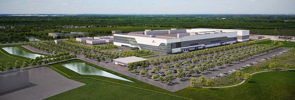
The facility focuses on advanced packaging for High Bandwidth Memory (HBM), which stacks multiple DRAM dies vertically through silicon vias (TSVs) to achieve the high-throughput, low-latency interconnects required by modern enterprise GPUs and AI accelerators. The Commerce Department agreed to a preliminary memorandum of terms in August 2024 covering up to $450 million in direct funding plus a loan of up to $500 million, and then finalized the award in December at up to $458 million in direct funding with the same loan ceiling. SK hynix has said the plant will make HBM manufacturing available in the United States for the first time, alongside a research partnership with Purdue.
The Korean Half of the Same Buildout
Indiana is the small end of what SK hynix is spending. On August 7, the company committed 54 trillion won, roughly $38 billion, to two new fabs at home: 35.2 trillion won for Y2 in Yongin and 19.1 trillion won for M17 in Cheongju. The split matters for what each one feeds. Y2 is a DRAM fab covering HBM and next-generation DRAM, while M17 is NAND, aimed specifically at enterprise SSDs and KV cache storage for AI inference. Neither arrives soon. M17 breaks ground in February 2027 with its first cleanroom in December 2028, and Y2 follows in July 2027 with a cleanroom in June 2029, with investment running into 2031.
Between Micron’s wafer agreement, SK hynix’s Indiana packaging plant, and these two Korean fabs, almost nothing lands before 2028. SK Group chairman Chey Tae-won, describing the current market to CNBC as “like a war” with everybody wanting to buy memory, said prices “went up too fast” and that the buildout is meant to help. He also framed HBM as moving away from commodity status, with NVIDIA and Google both wanting customized parts co-designed with their processors. NVIDIA has already locked in supply, securing HBM and agreeing to co-develop next-generation memory as part of a $500 billion arrangement with SK Group.
Indiana may not be the end of it. SK Group chairman Chey Tae-won told CNBC in August that the company had spent more than a month studying possible U.S. sites for front-end fab capacity, saying he is willing to build but still has to find the right place. Nothing is committed, and the Indiana plant remains packaging rather than wafer fabrication. For memory buyers, the two moves bracket the same problem from different directions. Micron is securing the raw substrate that feeds its fabs, while SK hynix is building domestic capacity for the packaging step that turns DRAM dies into the HBM stacks AI accelerators consume. Neither changes supply this year, and both are aimed at the back half of the decade.


 Amazon