

Samsung used the Future of Memory and Storage (FMS) 2026 conference to present its latest memory and storage technologies for artificial intelligence and high-performance computing. The company highlighted developments in DRAM, NAND, enterprise storage, advanced packaging, and semiconductor manufacturing.
Samsung’s opening keynote, titled “Driving the Wave of AI Revolution: 3D Innovations in Memory & Storage Architecture,” focused on using three-dimensional memory structures to improve system performance, power efficiency, and thermal management. Jin-Yub Lee, executive vice president and head of Flash Product & Technology, and Kyungryun Kim, vice president and project leader of the DRAM Design Team, discussed the company’s roadmap for future memory architectures.
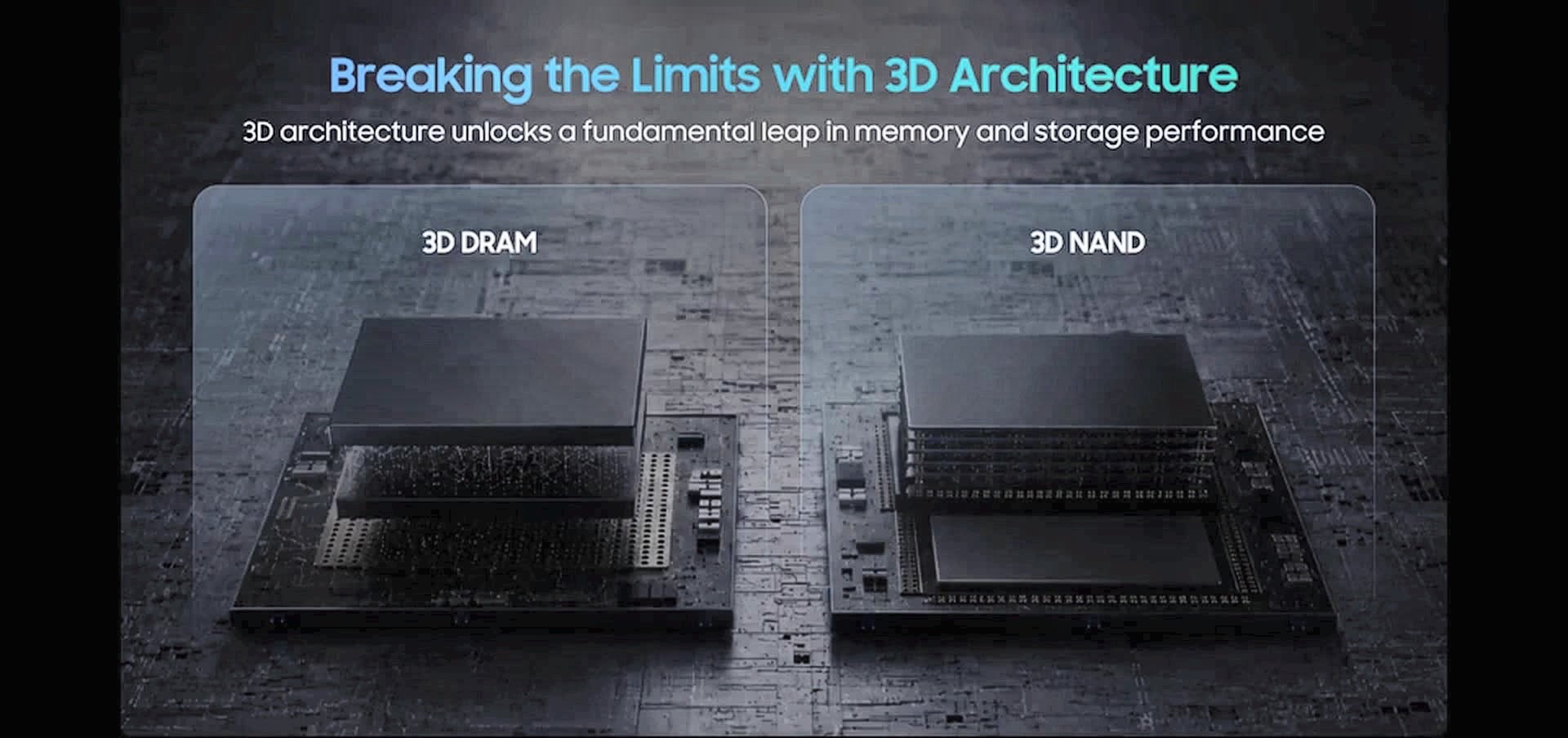
The company displayed about 30 technologies in a booth designed to resemble an AI cloud server. Key demonstrations included concept models for zHBM and zNAND-O, V10 Bonding V-NAND, HBM4E, HBM5, LPDDR5X-PIM, and enterprise SSD platforms including the PM1763 and BM1773.
zHBM Integrates Memory Directly Above AI Accelerators
Samsung presented zHBM as a future high-bandwidth memory architecture that vertically stacks HBM directly above an AI accelerator. This differs from conventional designs in which HBM packages are positioned beside the processor.
Placing memory closer to the accelerator reduces the distance data must travel. Samsung said the approach aims to increase bandwidth, reduce power consumption, and support data movement needs of large-scale AI training and inference.
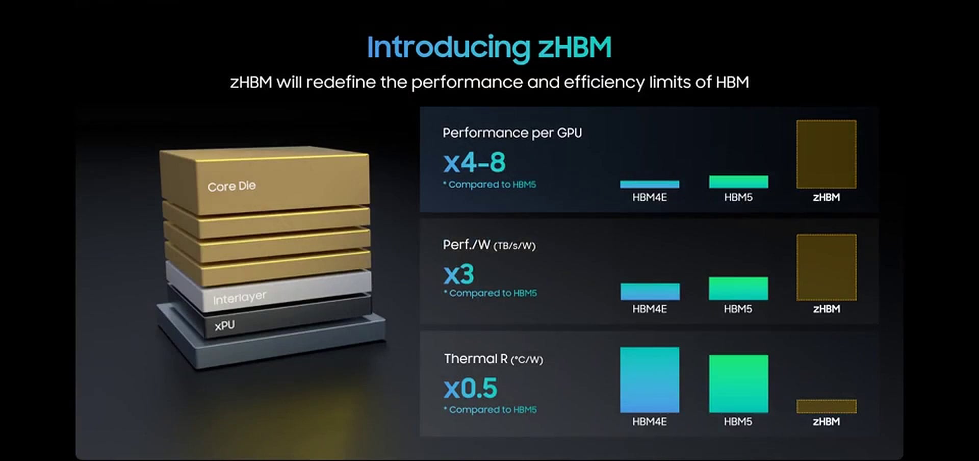
According to the company, an interface system using zHBM could deliver about eight times the performance of HBM5. The architecture is expected to provide over 10 times the memory density of HBM5, three times greater energy efficiency, and reduce thermal resistance by more than 50%.
zHBM is designed to support customer-specific configurations. Custom intellectual property could be integrated into the interlayer between the memory stack and AI accelerator, allowing system designers to tailor capacity and accelerator functionality for specific workloads.
zNAND-O Targets Edge AI Workloads
Samsung introduced zNAND-O, a high-performance NAND concept based on the company’s V-NAND technology. The architecture comes in four-layer and eight-layer configurations and is designed to improve space efficiency, I/O performance, and latency.
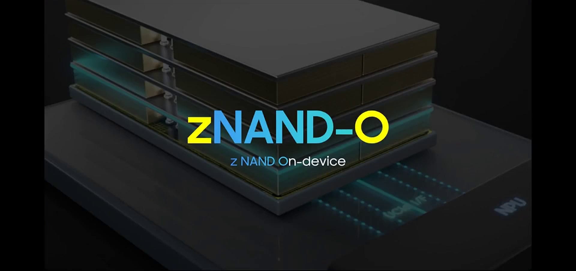
The company positioned zNAND-O for edge AI systems that process large datasets with minimal delay. By improving local storage performance, the architecture could support real-time applications where data cannot always be transferred to a centralized data center for processing.
V10 BV-NAND Moves Beyond 400 Layers
Samsung introduced V10 BV-NAND, a Bonding V-NAND architecture that uses wafer bonding technology to stack memory cells, unveiled as an industry first. The architecture stacks more than 400 layers, the highest Samsung has disclosed for its V-NAND line.
Samsung said V10 BV-NAND increases memory density by about 58% compared with V9. In addition to increasing capacity, the architecture aims to improve read, write, and I/O performance while reducing energy consumption.

The announcement comes 13 years after Samsung introduced the industry’s first V-NAND technology at the 2013 Flash Memory Summit. The company is targeting V10 BV-NAND for high-capacity, high-performance storage in future AI systems and other data-intensive applications.
HBM4E, HBM5, and LPDDR5X-PIM Extend the AI Memory Portfolio
Samsung presented HBM4E samples and an HBM5 model as part of its roadmap for next-generation AI accelerators. The company began the industry’s first mass production of HBM4, built on its 1c DRAM and 4 nm base die technologies, in February, and in May became the first to ship HBM4E samples to global customers.

The company also demonstrated LPDDR5X-PIM, which it describes as the industry’s first LPDDR memory with processing-in-memory technology. The design performs selected data-processing operations within the memory itself, reducing data movement between memory and processor. This can improve efficiency and lower power consumption for suitable workloads.
Samsung’s enterprise storage demonstrations included the PCIe Gen6 PM1763, which entered mass production in July, and the BM1773, both intended to support the growing storage requirements of AI data centers. These products complement the company’s memory roadmap by addressing the high-capacity and performance requirements associated with AI training data, model repositories, and inference workloads.
Samsung Promotes Integrated AI Infrastructure Development
Samsung positioned itself as the only integrated device manufacturer with capabilities spanning memory, foundry, and advanced packaging, presenting the combination as a one-stop platform for AI semiconductor development. The integrated model covers product design, semiconductor manufacturing, packaging, and mass production.
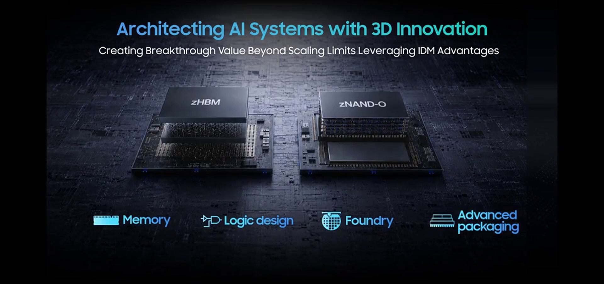
The approach aims to reduce the number of development stages between design and production while enabling tighter coordination between memory, processing, and packaging technologies. Samsung said this can help customers shorten development cycles and optimize performance and power efficiency for specialized AI systems.


 Amazon