

Sandisk and SK hynix have released the first HBF (High Bandwidth Flash) technical specification through the Open Compute Project, six months after the two companies formed the HBF workstream in February. Google and Tenstorrent joined the consortium during the standardization process, and the spec is now openly available to any company designing AI inference systems or accelerators.
HBF is a NAND-based answer to a DRAM problem. AI inference wants high-bandwidth memory close to compute, but HBM capacity is limited and expensive, while model sizes and context windows keep growing. HBF slots between the two extremes: flash-based stacks that trade some of HBM’s speed for far greater capacity and persistence, giving system designers a tier for model weights and long-context data that no longer fits in DRAM but cannot live on an SSD.
The specification puts real numbers behind the concept. Per SK hynix, HBF stacks come in 8-high and 16-high NAND configurations at up to 512GB per stack, with three performance grades spanning 0.4TB/s to 3.0TB/s, connected over the UCIe standard. The document defines the xPU-HBF host interface, electrical guidelines, baseline performance expectations, reliability and packaging guidance for an HBF die stack, and a software user guide for read and write operations. The companies designed the spec so HBF can coexist with HBM in the same system rather than replace it.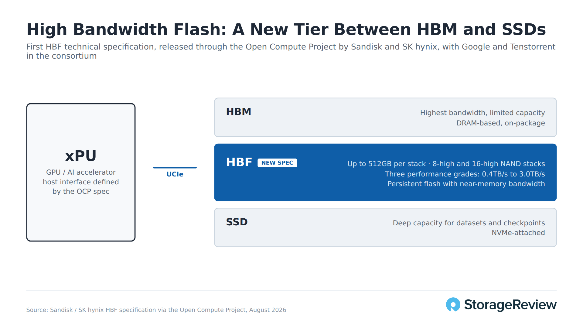
Sandisk and SK hynix are explicit about the strategy: publish early and openly through OCP to position HBF as the de facto standard for the AI storage market before rivals define an alternative. “AI inference is creating a new set of memory requirements, and HBF technology is designed to meet that moment,” said Alper Ilkbahar, chief technology officer at Sandisk, calling the spec a milestone “for the next generation of AI systems built to improve token economics at scale.” The capacity math is the same one driving KV cache offload to flash: keeping context in a cheaper, denser tier raises how many tokens and users each accelerator can serve.
BiCS10 QLC Claims the Density Crown
Sandisk’s other FMS announcement came with Kioxia: BiCS10 QLC, the pair’s tenth-generation quad-level-cell 3D NAND. The companies say the new die delivers a 60% bit density increase over their 8th-generation QLC and, at more than 37Gb/mm², the industry’s highest bit density for QLC NAND. It carries the same 332 active layers as the BiCS10 TLC die that began sampling in July, built on the same CBA (CMOS directly Bonded to Array) process that manufactures logic and memory array on separate wafers before bonding them.
On the interface side, BiCS10 QLC runs Toggle DDR6.0 at 4.8Gb/s with a Separate Command Address protocol, and adds Power-Isolated Low-Tapped Termination to improve data-out transfer efficiency. “Our 10th-generation QLC 3D flash memory delivers simultaneous gains in density, bandwidth, and energy efficiency,” Ilkbahar said, while Kioxia CTO Hideshi Miyajima pointed at the target market: efficiently storing rapidly expanding data volumes for AI systems. Neither company gave a sampling date for the QLC die.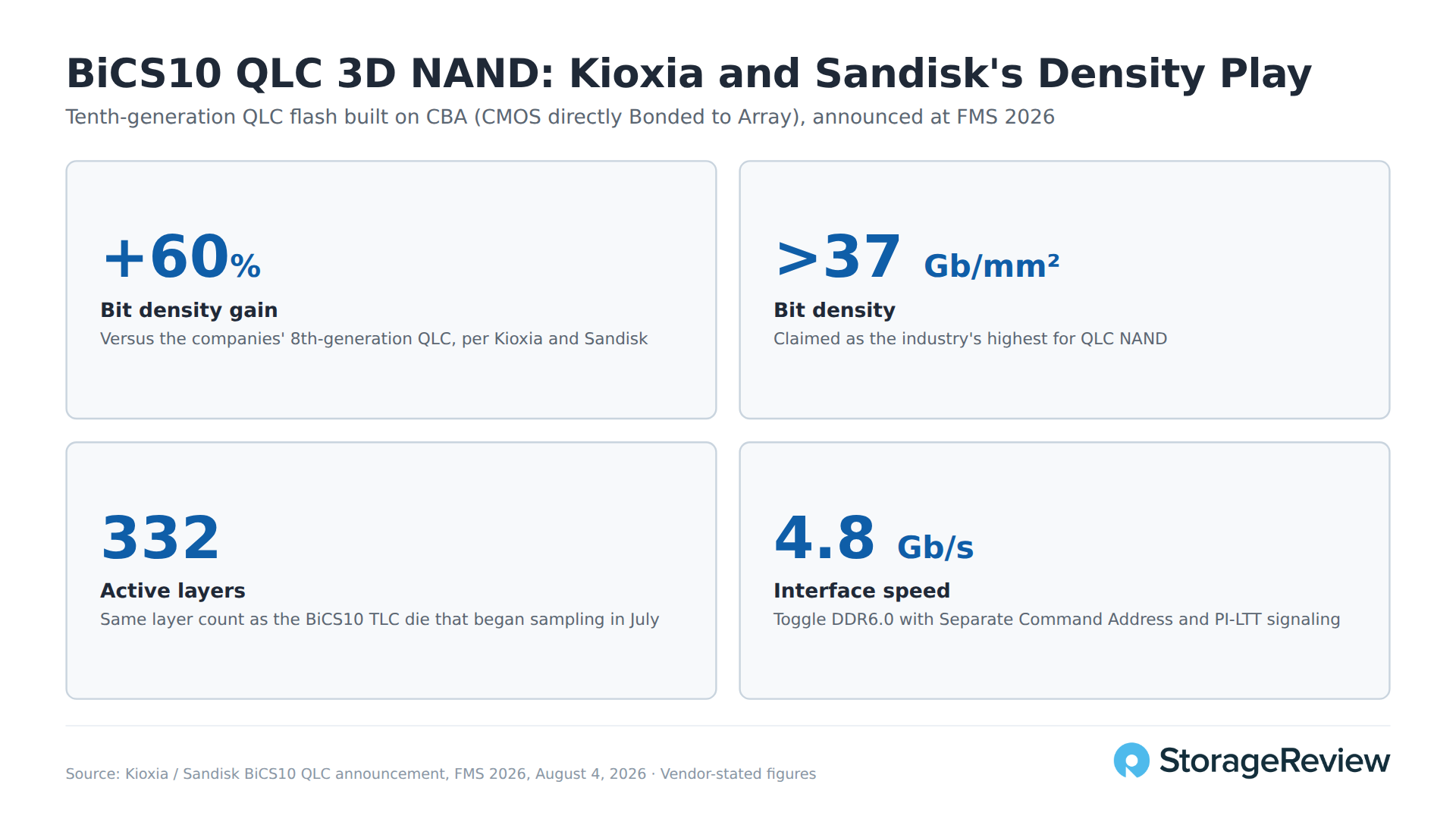
Keynote Wednesday, Memory Wall Panel Thursday
Sandisk’s FMS keynote, “NAND: The Versatile & Scalable Foundation of the AI Era,” runs Wednesday, August 5 at 11:40 a.m. PT, presented by chief revenue officer Jim Elliott, chief product officer Khurram Ismail, and Ilkbahar. On Thursday at 9:45 a.m. PT, Sandisk, SK hynix, and Google share a panel titled “Breaking the Memory Wall with High Bandwidth Flash,” moderated by Tom Coughlin, digging into architectural integration, standardization timelines, and the economics of the new tier. Sandisk is showing HBF, next-generation NAND, enterprise SSDs, and its updated AI Data Cycle framework at booth #607.
The spec release comes in a week thick with memory-hierarchy news; Samsung used its own FMS keynote to preview zHBM and zNAND-O concepts aimed at the same AI inference wall. The difference is that HBF now has a published, open specification behind it, and with Google and Tenstorrent already in the consortium, the standards race for flash-as-memory has a front-runner. All figures above are vendor-stated; we hope to see HBF hardware in the lab before anyone ships production systems built on it.



 Amazon