

Across several hardware generations, memory and networking vendors have identified different choke points in high-performance computing clusters. Memory manufacturers focused on in-package memory bandwidth, while network fabric providers addressed inter-chassis and cross-rack throughput. Today, those two perspectives have converged on the exact same bottleneck: the bandwidth wall that restricts data movement between distributed compute nodes and memory pools.
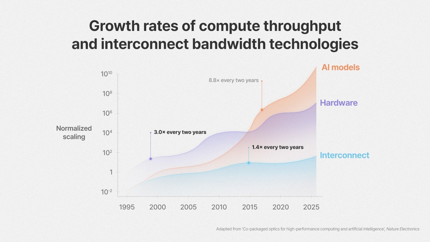
While High Bandwidth Memory (HBM) effectively resolved package-level bandwidth limitations for individual AI accelerators, modern hyperscale training and inference workloads now scale across tens of thousands of processors distributed across racks and pods. In these distributed topologies, computational throughput has historically increased by roughly 3 times every 2 years, whereas interconnect bandwidth has increased by approximately 1.4 times over the same period. The resulting imbalance places the primary scaling bottleneck squarely on the physical interconnect layer.
The assessment comes from a perspective paper published on August 20 in Nature Electronics, titled Co-packaged optics for high-performance computing and artificial intelligence, co-authored by SK hynix and researchers from the University of Virginia, the University of Illinois Urbana-Champaign, MIT, Nanyang Technological University, and Yonsei University. SK hynix AI Infra Team Lead Seunghoon Hong and UVA professor Kyusang Lee served as corresponding authors.
| Stage | Outcome |
|---|---|
| AI Cluster Scaling Bottleneck Shift | |
| HBM In-Package | Resolved on-die/package memory bottleneck |
| Copper Traces | Hits physical attenuation / power wall off-chip |
| CPO Integration | Converges the optical fabric directly onto the substrate |
To address this constraint, SK hynix, in collaboration with researchers from the University of Virginia, UIUC, NTU, MIT, and Yonsei University, published a study in Nature Electronics titled “Co-packaged optics for high-performance computing and artificial intelligence.” The paper details how co-packaged optics (CPO) and optical compute interconnects (OCIs) must co-evolve alongside memory and packaging architectures to sustain future cluster scaling.
The Physical Limits of Copper Interconnects
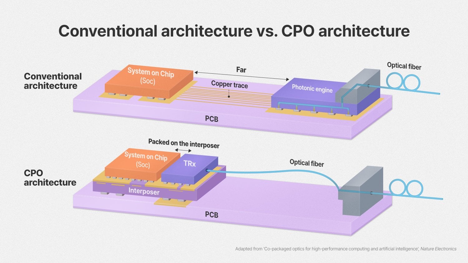
Standard electrical interconnects relying on copper traces and direct-attach copper cabling remain practical over short physical distances. However, as data rates increase, electrical signalling suffers from severe signal attenuation, insertion loss, and elevated power consumption. Managing high-speed signals across longer board traces and backplanes requires complex equalization and retiming circuitry, which introduces additional latency and consumes substantial power budgets.
How Co-Packaged Optics Changes the Path
CPO counters these physical limitations by mounting optical transceivers directly onto the same package substrate as the host processors or accelerators. Converting high-speed electrical signals to photonic channels directly adjacent to the compute silicon minimizes electrical trace lengths, mitigating parasitic capacitance and signal degradation. This architecture enables low-loss, high-bandwidth optical transmission across boards, racks, and pods while maintaining higher bandwidth density and improved immunity to electromagnetic interference.
| Metric | Target Specification |
|---|---|
| Target Specifications for CPO Nodes | |
| Node Bandwidth Density | > 100 Tb/s per node |
| Energy Efficiency | < 1 pJ/bit |
| Chip-to-Chip Interconnect Latency | < 10 ns |
| Integration Pathway | 2.5D interposer to 3D heterogeneous |
The roadmap projects an architectural progression moving from standard 2D multi-chip modules and 2.5D silicon interposer integration toward 3D heterogeneous stacking. The ultimate architectural milestone involves extending optical links directly into the memory subsystem itself.
By using a photonic interposer to directly interface memory stacks with compute engines, systems can bypass conventional board-level routing limitations. This approach enables disaggregated, low-latency shared memory pools where multiple compute engines can access shared capacity across an optical backplane without the serialization and deserialization penalties typical of traditional network fabrics.
Engineering Challenges for Commercial Deployment
Transitioning CPO from advanced packaging demonstrations into production data center hardware presents several unresolved engineering hurdles. Integrating low-power silicon photonic devices alongside high-power host logic demands sophisticated thermal isolation and advanced microfluidic or direct-to-package cooling designs.
Furthermore, the industry must develop standardized, low-latency coherence protocols capable of orchestrating optically coupled memory transactions without proprietary software overhead. Reliable commercialization will require end-to-end hardware co-design spanning DRAM die topologies, custom memory controllers, photonic engines, and heterogeneous substrate packaging. For SK hynix, the optical roadmap runs alongside its conventional one; the company detailed 16-High HBM4 and wafer-bonded 375-layer NAND at FMS 2026.


 Amazon